


Application
ELECTRICAL CHARACTERIZATION OF DIELECTRICS AND INTERFACES
Controlling electrical properties of dielectrics and the interfaces they form with semiconductors is imperative for achieving high IC device performance and yield. Semilab offers metrology solutions to electrically characterize the critical dielectric layers and processes that span process modules ranging from FEOL to BEOL.
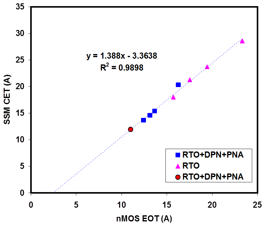
The most common implementation of Semilab’s in-line electrical metrology is replacement of the IC MOS short-loop, which alleviates the need for expensive and time-consuming processing. The in-line methods provide rapid feedback without the need for preparing devices; resulting in increased process tool utilization time for critical product. The two primary MOS measurements being replaced are; 1) Capacitance – Voltage (C-V) method for determination of Dielectric Capacitance, Dielectric Charges, and Dielectric/Semiconductor Interface Quality; and 2) the Current – Voltage (I-V) method that measures Dielectric Leakage and Breakdown.
The below table summarizes the dielectric properties measured by Semilab systems, the associated critical IC device parameters that are affected, and the process areas in which the issues are commonly encountered.
Measured properties of dielectrics and interfaces:
| Measured Property | Affected Device Parameter | Process Module | |
|---|---|---|---|
| Dielectric/ Semiconductor Interface Quality (Dit, Qit, Nit) | Threshold voltage (Vt), Carrier Mobility, Reliability/ Hysteresis | Diffusion, Gate, Cleaning, |
ILD Plasma Thin Films |
| Dielectric Charge (Qf, Qm, Qot, Vfb) | Vt, Reliability/ Hysteresis | Diffusion Gate |
Plasma Thin Films |
| Dielectric Capacitance (CD, CET, EOT) | Vt, Reliability/ GOI, RC | Diffusion Gate |
ILD Thin Films |
| Surface Charge (VPDM, NVD, Vsurf) | Reliability/ GOI | Cleaning Plasma |
Thin Films Ion Implant |
| Dielectric Leakage (I-V, I-E, SILC, Etunnel) | Reliability/ GOI | Diffusion Gate Cleaning |
ILD Plasma |
In order to meet the individual requirements of our diverse customer base, Semilab offers various versions of these techniques using multiple approaches; including the non-contact Corona-Kelvin method and the contact methods using Elastic Metal Probe (FCV system) and Mercury Probe (MCV system).
Technology
ELASTIC METAL PROBE C-V PROFILING
Elastic Metal Probe C-V Profiling makes rapid measurement of electrical parameters associated with dielectrics including gate oxides or near-surface resistivity of epitaxial layers. This method provides a very effective solution for in-fab process monitoring or product certification of product wafers.
Elastic Metal Probe C-V Profiling is a very effective technique for measuring the electrical properties of dielectrics, pn-junctions, Si and GaN epitaxial layers on either bare or patterned wafers. Using the patented EM-probe technology, measurements are performed without chemical treatment, eliminating mercury contacts and damage or contamination on the wafer surface.
Semilab FCV systems use a small elastic probe to form a temporary gate on the dielectric surface.
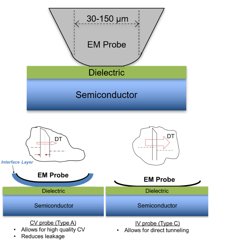
There are two types of Elastic Material Probes (EM-Probes) that are used. Type A probe (on the left) is used for all CV and GV and surface resistivity measurements. It has a self-contained dielectric on the probe surface that blocks direct tunneling currents and allows for leakage free CV measurements on ultra-thin dielectrics. For IV measurements, a type C probe is used (on the right). This probe uses a unique metal that does not readily oxidize and whose oxide is conductive rather than insulating.
MEASURED PARAMETERS FROM CV CURVE:
- Capacitive Effective Thickness (CET)
- Equivalent Oxide Thickness (EOT)
- Density of Interface State (Dit)
- Flatband Voltage (Vfb)
- Changing of Flatband Voltage (Delta Vfb)
- Threshold Voltage (VT)
- Average Surface Doping (Nsurf)
- Surface Resistivity (ρsurf)
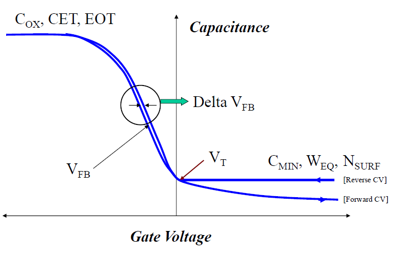
FCV forward and reverse CV curves. The key CV based parameters are shown in the figure.
FEATURES
- In-line monitoring of dielectrics and epi resistivity on product wafers
- No mercury contact and non-damaging, non-contaminating probe permits wafer reuse
- Hard probe for patterned wafers with metal pads
- Elastic Material probe for non-damaging and non-contaminating measurement on bare or pattern wafers
Product Line
FCV
Gate dielectrics characterization and resistivity monitoring with site-based measurements
(typically 5 or 9 points per wafer according to SEMI standard testing patterns).
Specially designed probe ensures that no damage is done to the wafer, because the probe is not contaminating the wafer surfaces.
Products

FCV-3000N Modular CV/IV Metrology System
FCV-3000N Modular CV/IV Metrology System is a solution for in-line monitoring the quality of dielectrics and epitaxial silicon product wafers of the memory and power device industries with non-destructive contact measurement method. The optional pattern recognition system locates scribe line test areas on patterned samples.
The system contains a class 1 mini-environment and meets applicable SEMI and CE standards.
FCV system can be confugured with
- a small elastic metal probe to form a temporary gate on the dielectric surface of bare or patterned samples, or
- a hard probe, which provides electric contact to metal test pads on patterned wafers.
Features and System specifications:
- Elastic metal probe does not damage the dielectric surface
- Hard metal probe for 1-pin measurements and a hard metal probe pair for 2-pin measurements are also available which gives a more precise positioning.
- Measurements down to 1 mm edge exclusion
- One or dual load ports
- Automated wafer handling for 200 and 300 mm wafers
- OHT capability option
- Easy to learn and use SAM User Interface running under Windows-based operation system
- Easy transfer of data over fab networks with common networking software.
Probe movement, wafer motion, cassette loading or uploading, and wafer pretreatment are controlled by an internal computer according to user-defined stored recipes.
Measurement Capabilities:
- C-V measurement
- I-V measurement
- Ramped Current Stress Test (RCST)
- Constant Current Stress Test (CCST)
- Ramped Voltage Stress Test (RVST)
- Constant Voltage Stress Test (CVST)
Request Info