


Semilab presents the En-Vision
05.26.2017
We are pleased to present En-Vision (Enhanced Vision), a new generation inspection system specifically targeting quick and non-destructive detection of nm scale buried defects.
Buried defects are located under the silicon surface, invisible to conventional inspection tools (Optical / SEM), and when occuring in the active areas impact device performance and yield.
Facts
- Buried defects such as dislocations, COP’s or Oi precipitates may cause severe yield issues when located in active device areas.
- Previously only destructive methods could identify such defects.
- Time consuming (weeks).
- Provide only partial information (high uncertainty).
- Buried defects (process and stress-related) are most critical during the ramp up and yield optimization phases for a new product.
Benefits
- Non-destructive in-line detection of buried defects in FEOL.
- En-Vision dramatically speeds up the detection of buried defects.
- Faster manufacturing ramp up and yield enhancement.
- Save time and resources for detection and investigation of buried defects.
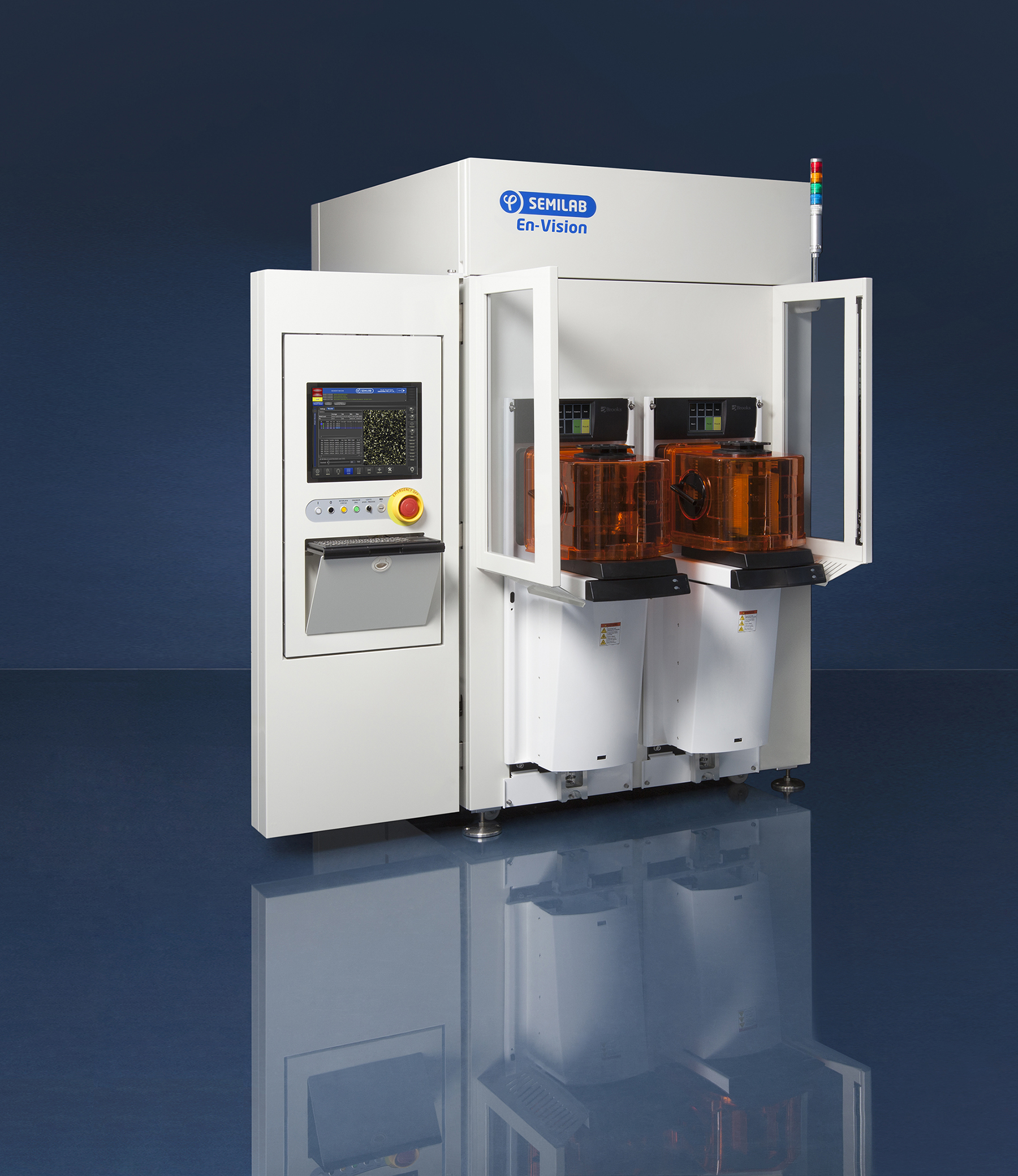 Figure 1. En-Vision
About Semilab
We design, produce and sell metrology equipment for the characterization of semiconductor and photovoltaic materials, for monitoring the manufacturing process of semiconductor devices and solar cells, and also for R&D purposes in these areas. We offer a variety of measurement techniques; most of them are non-contact and non-destructive. Many of our technologies can be flexibly integrated into different platforms, ranging from simple handheld devices and table-top systems with high resolution mapping capability to fully automated stand-alone production control tools for mid-range and high-level fablines. We also offer in-line measurements for solar cell production lines.
Our strategy is to continuously improve our products, and to offer flexible solutions for our customers’ needs with high-value products for a reasonable price.