


Application
NANO SURFACE CHARACTERIZATION
The topographical features of the surfaces in the semiconductor industry are an important source to gather information about possible failure sources or estimate success rates to improve the overall yield of the process. Therefore the investigation of the smallest surface features of silicon substrates, as well as patterned wafers can be found in a lot of applications throughout the industry.
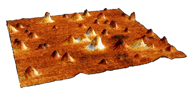 Figure 1. Surface features