


Application
INLINE PROCESS CONTROL
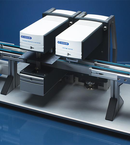
Besides Semilab’s own automated wafer sorter platform, Semilab manufactures separate measurement units for integration into automated PV production lines. Semilab has been working together with all the relevant automation companies to integrate the measurement units.
The equipments cover a diverse range of metrology needs for comprehensive process and quality control in Si PV industry:
- Incoming wafer inspection and process control during cell manufacturing
- Measurement in as-cut wafer, textured, after diffusion, after passivation, after ARC deposition, after contact formation states
- Measurements of geometrical, electrical and optical properties
- Solutions for mono and multicrystalline silicon materials, Al-BSF, PERC, IBC and heterojunction cell concepts
All measurement units are designed considering the following directives:
- Compatibility to state-of-the-art production lines
- Supporting all the industry standard communication protocols
- Flexible integration
- Supporting both „on-the-fly” and „stop-and-go” data acquisition modes
- Compact design
- Simple integration and support
- Simple maintenance, rare calibration periods
- Application of noise reduction solutions
- Simple and configurable customization of communication protocols
Technology
PHOTOLUMINESCENCE IMAGING
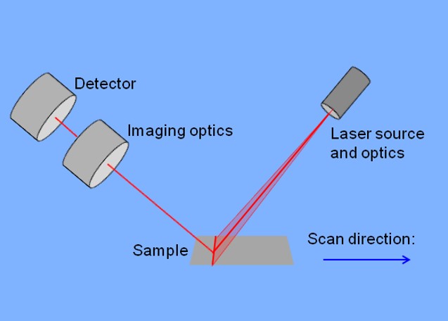
Photoluminescent Imaging is an excellent tool for monitoring of multicrystalline, monocast or monocrystalline wafers. During the measurement, the laser illuminates the silicon block and the generated photoluminescent signal is detected by an IR camera. The illumination effects the recombination of charge carriers. If not, the defects are present and there is a chance of radiative recombination. During the radiative recombination, a photon is emitted which can be detected by an IR camera. PL intensity is inversely proportional to defect density and impurity concentration.
System features:
- High quality fast imaging even for as cut wafers
- Advanced on-the-fly lifetime calibration method
- Flexible classification according to the particular requirements
- Detection of wafers with broken edge
- Capability to measure solar wafers at any processing stage providing full process control
- Accurate tool matching capability
- Cell efficiency forecast capability at as-cut stage
- Flexible configurability from stand-alone to integration in fully automated systems
TYPES OF DETECTABLE DEFECTS:
1. Material (as-cut wafers):
General
- High contamination density
- Edge (corner) contaminations
Multi wafers
- High dislocation density
- Active grain boundaries
Mono wafers
- Ring defects (for different reasons)
- Pinholes
- Cracks
2. Passivation control (double side passivated samples)
Optional on-the-fly Jo and iVoc mapping
3. Wiring (finished cells):
Shunt
Edge isolation defect
Bad finger
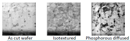
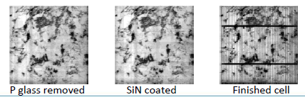
PL IMAGES AT DIFFERENT PROCESSING STAGES:
COMPARISON OF PLI AND LIFETIME FEATURES:
Good correlation between PL and μ-PCD data allows calibration between PL intensity and lifetime:
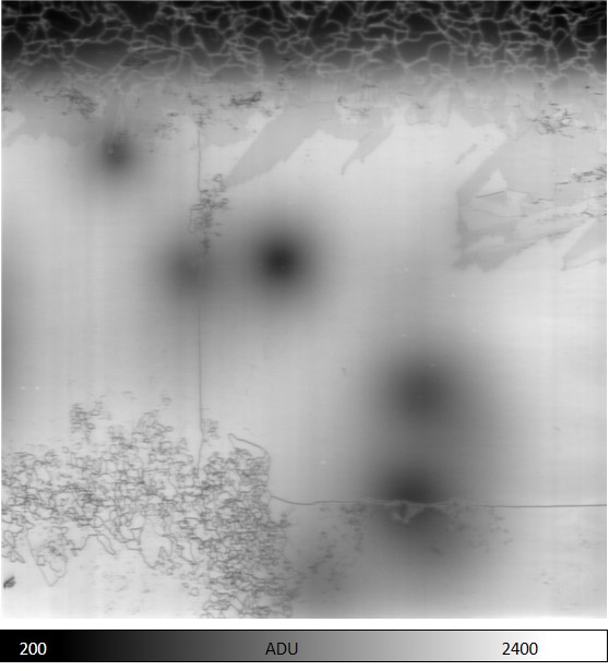
PL image
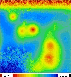
μ-PCD image
Point-to-point correlation of Multicrystalline wafers with lifetime:
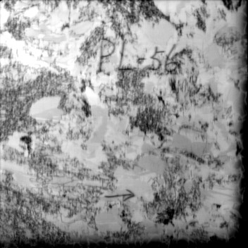 PL image
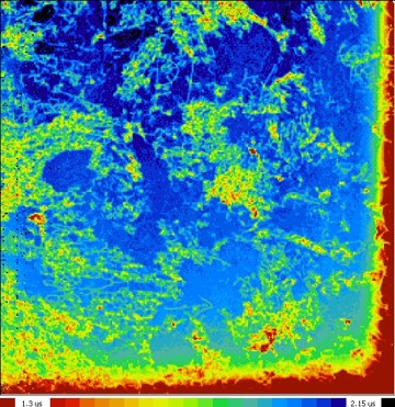
μ-PCD image
CORRELATION BETWEEN FORECASTED AND MEASURED CELL EFFICIENCY
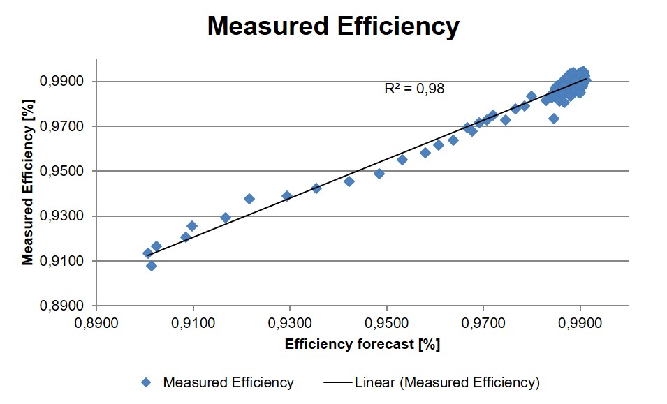
Semilab’s sorting solution provides good consistency between multicrystalline wafers and efficiency of final cells.
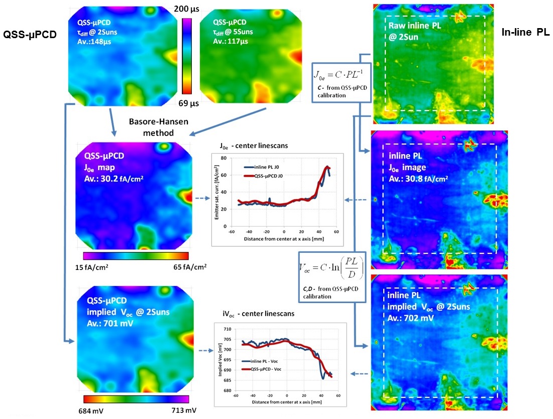
COMPARISON OF J0 AND IMPLIED VOC MAPPING BY QSS µ-PCD
FEATURES
- Reflection side photoluminescence on finished cells, processed and as-cut wafers
- On the fly lifetime map from µ-PCD calibrated PL image
- Applicable for R&D usage
- Quality description by calibrated lifetime map and customizable classification parameters
- Cell efficiency forecast from PL images as-cut multi/monocast wafers (calibration required)
- Measurement capability both on slurry and diamond-cut wafers
Product Line
PLI
Photoluminescence tool for wafer and cell inspection is a fast and reliable solution for non-destructive measurement of wafer and cell quality at any stage of processing from as-cut wafers to finished cells.
Provides full control of material quality during the whole production.
Higher quality wafers create higher efficiency cells making the production more cost-efficient.
Products

PLI-101/A, PLI-103/A
Photoluminescence tool for wafer and cell inspection
Inline photoluminescence tool is a fast and reliable solution for non-destructive measurement of wafer and cell quality at any stage of processing from as-cut wafers to finished cells.
Provides full control of material quality during the whole production.
Higher quality wafers create higher efficiency cells making the production more cost-efficient.
Features and System specifications:
- Fully automated inline photoluminescence imaging and inspection
- Reflection side photoluminescence on finished cells, processed and as-cut wafers
- On the fly lifetime calibration
- Quality description by calibrated lifetime map and custom classification parameters
- Sample size: PLI-101/A up to 156 mm
- PLI-103/A up to 162 mm
- High equivalent in-line throughput
Types of detectable defects:
PLI-101, PLI-103
Material:
- High dislocation density
- Cracks
- High contamination density
- Edge (corner) contaminations
- High vacancy density (for mono wafers)
- Low lifetime
PLI-101, PLI-103
Wiring:
- Shunt
- Edge isolation defect
- Bad finger
PLI-101A, PLI-103A
Passivation control (double side passivated samples)
- Optional on-the-fly Jo and iVoc mapping
We offer automated PLI-200 version as well.
Request Info