


Precision Measurement Tools for the Sub-Nanoscale
08.15.2023

The advancement in precision measurement tools has revolutionized how scientists delve into the intricacies of sub-nanoscale material properties. Both contact and non-contact methods have improved by orders of magnitude over the systems of previous generations. Nanoindentation, for example, enables the interrogation of various mechanical properties by observing extremely small-scale deformations in response to a controlled load. Meanwhile, atomic force microscopy (AFM) offers high-resolution 3D surface analysis by scanning a sharp probe across a sample’s surface.
This blog post focuses on spectroscopic ellipsometry (SE), a non-destructive precision measurement tool employed to unravel the characteristics of various materials. Here, we’ll focus on SE's role in investigating the growth of thin film molybdenum carbide (MoCX).
Spectroscopic Ellipsometry in Thin Film Characterization
The novel development of Plasma-Enhanced Atomic Layer Deposition (PEALD) facilitates the synthesis of atomically thin continuous MoCX. Researchers can accurately measure the initial film growth rates by employing real-time in-situ spectroscopic ellipsometry.
The unique characteristic of SE lies in its wide wavelength range (245 to 990 nm), which enables accurate measurement of film thickness at the sub-nanoscale.
Additionally, SE is indispensable in identifying the optical properties of the MoCX, which can alternate between conducting and semiconducting characteristics.
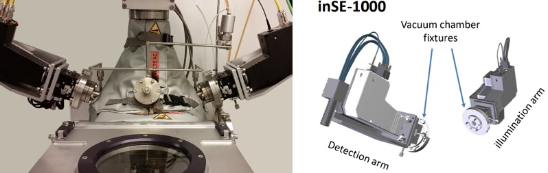
Figure 1. Real time in situ spectroscopy for PE-ALD processing with a sampling rate of <0.2 ms per measurement for 245 – 990 nm wavelength.
The Experimental Framework
The PEALD-grown MoCX film experimentation occurred in a top-flow, PE-ALD reaction chamber. Notably, hydrogen plasma was pivotal in the experimental framework by removing the adventitious organic contamination on silicon surfaces. In this way, it aided the removal of native SiO2 oxide, serving as a precleaning step for thin film depositions.
Probing the Growth Mechanism with Plasma Pre-Treatment
Plasma pre-treatment using H2/Ar plasma offers observable changes in native oxide, marking the removal of adsorbed organic components. This methodology provides vital clues about the growth mechanisms during the initial MoCX PE-ALD cycles. Such findings add significantly to our understanding of precision measuring tools at the sub-nanoscale level.
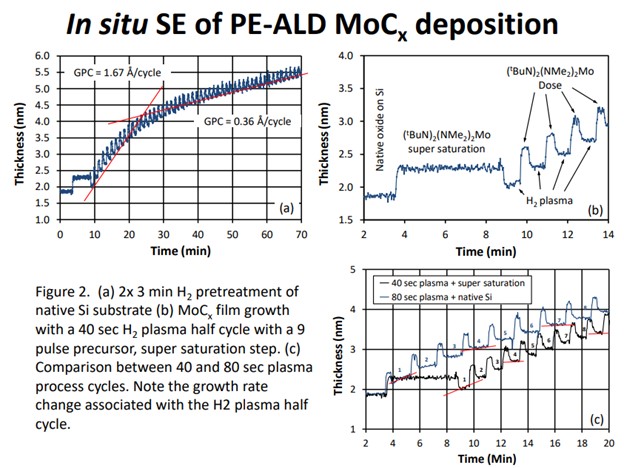
Image Reference: In Situ Characterization of Thin Film Molybdenum Carbide Using Spectroscopic Ellipsometry. A. Bertuch, J. Hoglund, L. Makai, J. Byrnes, J. McBee, G. Sundaram. Veeco - CNT, SemiLab USA.
From Initial Cycles to Steady State
The interaction of the plasma with the substrate contributes to the evolution of the film growth. After about seven to eight cycles, the observed slope during the plasma step effectively reduces to zero. This finding emphasizes the need for precision in the monitoring and controlling of PE-ALD process, a task achievable through real-time in-situ spectroscopic ellipsometry.
Unlocking Insights with Real-Time In Situ Spectroscopy
The essence of real-time in situ spectroscopy lies in its capacity to provide immediate and in-depth feedback during a specific process. By enabling real-time monitoring, it offers researchers unprecedented control over the process based on the spectroscopic data obtained. It is particularly useful for thin film characterization, deposition or etch process monitoring, and materials quality control.
The power of precision measuring tools lies in their capacity to provide insights that enhance our understanding of sub-nanoscale processes. We can refine our methodology by using real-time in situ spectroscopy, making strides in materials science, surface science, and thin film technology. With the continued exploration of spectroscopic ellipsometry, we remain at the forefront of innovation, pushing the boundaries of scientific exploration.
At Semilab, we strive to foster progress in the scientific community through innovation. As we delve into spectroscopic ellipsometry and other precision measuring tools, we invite you to explore our range of products and research today.