


Tailored Surface Characterization Tools for R&D
09.25.2023

In research and development (R&D), surface characterization plays an essential role in understanding complex relationships between the processing, structure, properties, and performance of advanced materials. The analysis of surface properties, including morphology, chemistry, energy, and nanomechanical properties, is required to obtain deep insights into material behavior. As a result, tailored surface characterization tools have emerged as invaluable assets for scientists and engineers engaged in R&D projects. This article will highlight the importance of surface characterization in R&D and explore the benefits of using tailored surface characterization tools for improved productivity and a competitive edge.
Tailored Surface Characterization Tools
Tailored surface characterization tools enable scientists and researchers to obtain in-depth information about the properties and behavior of materials. By making the most of these tools, R&D professionals can gain invaluable insights and drive innovation. Several types of tailored surface characterization tools are available, each with its own advantages and disadvantages. Some primary examples include:
Nanomechanical Methods
Nanoindentation and related techniques assess the mechanical properties of material surfaces, including hardness, elastic modulus, and adhesion. This is achieved by measuring a material’s mechanical response to a controlled load using displacement sensors. A nanoindenter like the Semilab IND-1500 offers in-depth assessments of the mechanical measuring properties of material surfaces. By measuring parameters such as hardness, elastic modulus, and adhesion, nanoindentation provides crucial insights into material strength and durability.
Scanning Probe Microscopy
Scanning probe techniques like electrostatic force microscopy (EFM), atomic force microscopy (AFM), and scanning tunneling microscopy (STM) offer detailed assessments of surface morphology and electronic properties at the nanometer scale. These methods are particularly useful for examining surface structures and defects as they allow the precise measurement of surface topography and roughness.
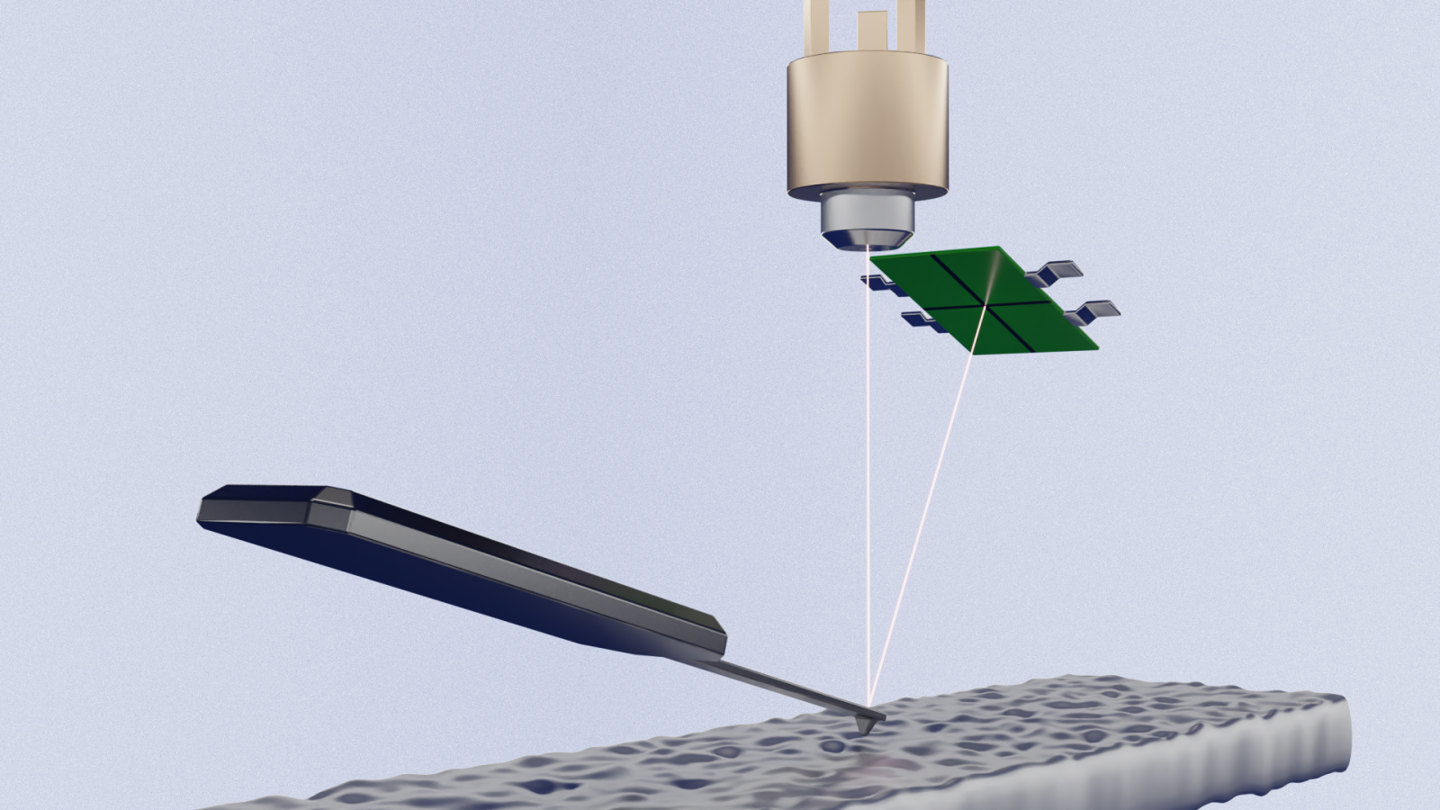
Figure 1. Illustration of an AFM setup. The tip-sample interaction force is detected by focusing a laser on top of the cantilever and measuring the position of the reflected beam.
One to Focus On: Atomic Force Microscopy
Atomic force microscopy is a crucial method because it can reach lateral atomic resolution, thus providing exact details on the electrical and mechanical properties of a surface, as well as topography.
Having a tool that can measure almost any surface is invaluable in a wide range of applications. It is used in chemistry to analyze the properties of electrochemical cells and in microelectronics to characterize semiconductors. Another benefit of AFM is its use in research and development. It supports experts working with flat panel displays, thin films, semiconductors, and materials science, focusing heavily on surface characterization.
AFM can also be combined with scanning electron microscopy (SEM), which creates tandem benefits. The AFM component provides highly sensitive height information – excusive to the top layer of atoms on the surface. Meanwhile, the SEM aspect assists with precise positioning of the AFM probe’s tip plus in situ monitoring of tip condition and sample manipulation.
Surface Characterization Systems from Semilab
Surface characterization is paramount in research and development activities, enabling scientists and engineers to learn more about advanced materials, resulting in improved productivity and a competitive edge. At Semilab, we offer a range of tools to enable surface characterization, including a stand-alone atomic force microscope and a solution that can readily be integrated into SEM-AFM configurations to suit scientists in multiple disciplines.
We have developed the Semilab AFM series for academic and industrial use. This series was designed to help users achieve the best and most reliable results as quickly as possible.
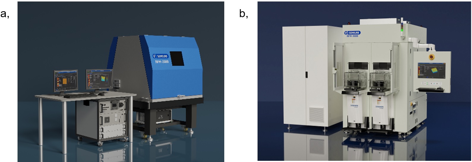
Figure 2. Semilab AFM series including a, manual AFM and b, automated AFM.
Our automated AFM systems can be integrated with our proprietary μPIT metrology for micro particle inspection, which enables efficient defect localization, streamlining the defect review process and enhancing the overall efficiency of surface characterization. Our instruments are compact and allow for total visual control thanks to the integrated optical axis fitted. In addition, it offers low noise and a high-resolution digital CCD camera.
Contact a member of Semilab today to learn more about tailored surface characterization tools in research and development.
Interested in surface characterization? Check our infographic!
https://semilab.com/en/news/pushing-size-limits-in-the-semiconductor-industry-and-metrology