


Application
THIN FILM OPTICAL CHARACTERIZATION
Thin film (ITO, OLED, LTPS, IGZO, SiNx, SiOx, photoresist, etc.) thickness and optical properties is one of the key process control parameters. Using Spectroscopic Ellipsometer of Semilab fast (measurement speed is similar to reflectometers) and accurate measurement can be performed at any size of the panel.
Using our advanced analysis software, the following parameters can be determined as well: optical band gap energy, transmission, roughness, crystallinity related parameter (in case of LTPS).
SiOx/Glass structure can be a challenge to measure using conventional optical metrologies, however due to the principle of ellipsometer used in FPT even such low contrast structures can be measured accurately.
.png)
Technology
SPECTROSCOPIC ELLIPSOMETRY
In the semiconductor industry, there is continuous demand for higher performance and denser integrated circuits. These requirements push the advancement of technology which requires solving of manufacturing challenges. A key to success is to understand the chemical, mechanical and physical properties of wide range of materials used in a typical integrated circuit.
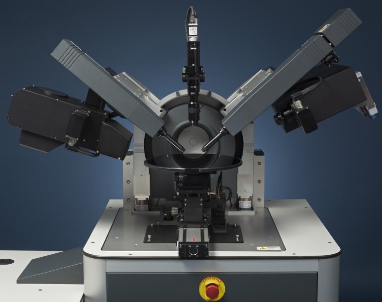
The µSE tool is designed to measure thin film thickness and optical properties inside a <50µm test pad on semiconductor product wafers. The applied measurement technique for obtaining these parameters in a high accuracy and repeatable way is spectroscopic ellipsometry. The μSE tool uses optimized spectroscopic ellipsometer (SE) arms and optics for the measurement inside small boxes of patterned Si wafers.
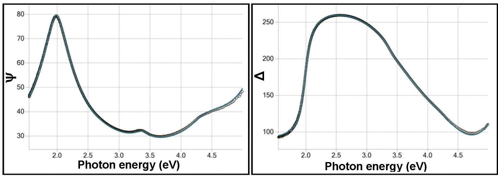
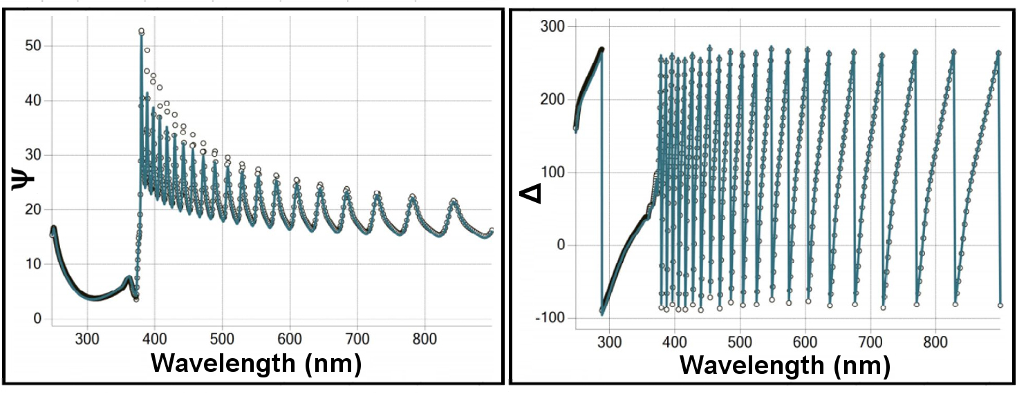
Ellipsometry measures the phase of the reflected light from the sample, therefore it is relatively insensitive for intensity fluctuations. The raw measurement data represent the complex information from the layer stack which then need to be modeled optically. The measurement results are obtained through numerical regression process of the model data to the raw measurement spectrum.
TYPICAL SE REGRESSIONS:
FEATURES
- Non-destructive optical technique, based on measurement of the change of the polarisation state of light after reflection at non normal incidence on the surface to study.
- It is a higly sensitive even for layer thickness below 5 nm
- Extremely versatile technique: it gives acccess to numerous parameters which characterize multilayer structures (eg. layer thickness, refractive index, absorption, porosity).
Product Line
SE, inSE, R2R SE
Refractive optical design in compact realization: short optical path inside the measurement arms (reduced alignment artifact errors). Active temperature control: stabilized environment for system reli-ability enhancement. Uniqe patented high brightness light source for outstanding SNR. CCD detector array (spectrum is taken simultaneously at different wavelengths).
Products

SE-2000 Spectroscopic Ellipsometer
SE-2000 features the widest spectral range available on a single tool. The ranging is from the deep UV (190 nm) up to mid-IR (25 μm). The tool is uniquely offered with an optional FTIR ellipsometer head on the same goniometer with the visible arms. It can be configured with the fast detection mode by using spectrograph and detector array, with the high resolution mode by using spectrometer and single point detectors, or with both modes together on the same tool. SE-2000 includes Semilab’s new smart electronics with interchangeable components, and operates with the new generation operating and analysis software (SAM / SEA). The system can be controlled from a PC or laptop through LAN network, or by a new touch panel interface.
Measurement modes:
- Spectroscopic Ellipsometry for thin film thickness and optical functions, including complex multilayer structures
- Generalized Ellipsometry for anisotropic materials
- Transmission Ellipsometry for transparent substrates
- Scatterometry vs. wavelength and angle of incidence
- Mueller Matrix (11 or 16 elements) uniquely offered in combination with Scatterometry for 3D anisotropic materials
- Jones Matrix for simple anisotropic materials
- Reflectance & Transmittance vs. wavelength and incidence angle
- Polarimetry
- Porosimetry: Measurements of pore size and porosity in thin films
- In situ measurement mode for real time control during deposition or etch process
Options:
- Mapping stage (X, Y, Z, rotation), manual or automatic
- Microspot (standard and ultra small - customization is subject to discussion)
- Environmental cells: cryostat, liquid cell, cooling and heating sample stage cells, QCM cell
- Atmospheric porosimetry chamber
- Visualization camera
- Spectroscopic Reflectometer
- Extended spectral range detection
- Possibility of integration of other Semilab metrologies (4pp, Eddy, etc.)
Request Info


inSE-1000 In-Situ Spectroscopic Ellipsometer
The new in-situ thickness measurement system, inSE-1000 provides instant access to layer thicknesses and optical properties through ellipsometric specra analysis during layer deposition processes in vacuum chambers and load locks.
inSE-1000 is the part of Semilab's ellipsometry tool family specially designed for the measurement on vacuum chambers during deposition or treatment processes or in load locks. The easily mountable arms can be placed on the vacuum chamber or on an offline testbench for detailed investigation of the final product. The electronic components and supplementary systems are situated in a cabinet, which can be placed next to the deposition tool. The ethernet interface allows on-demand measurement sequence with the deposition tool and the two-way communication protocol.
Features and system specifications:
- CF-40 vacuum port interface
- 75 W, short arc Xenon lamp by optical fiber
- Rotating compensator optics
- Beam divergence < 0.2o ( in parallel beam, no focusing)
- Compact arms
- Spectral resolution for fast mode
Software:
- Immediate visualization of the measurement data and the fitting results: thickness and optical properties
- Modelling of each layer with all known methods including dispersion laws, alloy model, periodic layers, phase node model, anisotropic layer evaluation, or user-defined free formula
- Ethernet-based communication protocol with the deposition tool computer
- The largest (n, k) database
Request Info
")
SE-2000-IR Spectroscopic Ellipsometer (IR)
SE is traditionally used in the UV/visible/near-infrared wavelength region (190-2500 nm) for precision metrology of layer thicknesses, refractive indices and alloy concentrations. Semilab proposed a Fourier Transform Infrared Spectroscopic Ellipsometer (SE-2000-IR) for research and development. Infrared region is interesting, because in many cases absorption bounds related to the chemical composition of the sample can be detected. Thickness information can also be gained from the infrared region from interference fringes as in the UV-visible region. Moreover, free carrier concentration affects the absorption coefficient in the infrared range giving a non-destructive way to measure this parameter using the Drude tail.
Request Info
R2R SE - Roll-to-Roll Spectroscopic Ellipsometer
Immediate determination of film uniformity and homogeneity are important factors for in situ coating quality process control. Spectroscopic Ellipsometry (SE), as a measurement method ensures fast and reliable measurement required by characterization of thin film coatings on thin foil substrates. Semilab’s novel R2R SE metrology platform offers multilayer thickness and refractive index determination directly after the coating process on a moving roll-to-roll foil on-the-fly with acquisition time less than 100 ms per point.
Features and system specifications:
- Fast and accurate analysis of multilayer coatings - feed forward functionality in the evaluation
- Sequential (step-by-step) evaluation of only one layer at a time, without the need of performing the full stack analysis.
- Elimination of the stray light reflected from the backside of the transparent substrate
- Spot size: 500 μm at 633nm
- Spectral range: VIS/NIR
In-line control:
- Reflectance
- Layer thickness
- Ga-content (CIGS)
- Conductivity (TCO)
- Roughness
Request Info


EPA or Vacuum Porosimetry extension for SE-2000 Spectroscopic Ellipsometer
The EPA (Ellipsometric Porosimeter Atmospheric pressure) is designed to allow fast film characterization at ambient pressure and temperature. To make mesopore size investigation simple, cheap, and non toxic, we performed EP measurements using a pulsed air flow with controlled partial pressure of water. This system allows a fast partial pressure equilibration at each point of the isotherm (a complete adsorption-desorption cycle can be obtained within 30 min time)
The EPA setup is made of a spectroscopic ellipsometer on which is fixed a cell of environment control containing the film to analyze. In laboratories, gas volumetry analyses are usually time-consuming, mainly because of long pressure equilibration time within the analysis chamber. In the experimental setup of these experiments, we replaced the pressure equilibration system by a continuous flux of air containing a fixed partial pressure of adsorbate directly in contact with the mesoporous film to analyze.
EPA gives access to:
- Pore size Distribution from 1.5nm to 60 nm diam
- Average pore size
- Porosity
- Cumulative surface area
- Thickness – refractive index – absorption coefficients
- Young Modulus

SE-1000 Spectroscopic Ellipsometer - Tabletop Manual System
SE-1000 provides modularity and high measurement performance in a compact table top footprint. This cost-efficient tool includes manual goniometer and manual sample positioning suitable for R&D laboratories. It performs non-contact and non-destructive optical measurements on substrates, single layer and multi-layer samples to obtain individual thin film thickness and optical properties. SE-1000 includes Semilab’s new smart electronics with interchangeable components, and operates with the new generation operating and analysis software (SAM / SEA). The system can be controlled from a PC or laptop through LAN network, or by a new touch panel interface.
Measurement modes:
- Spectroscopic Ellipsometry with rotating compensator
- Generalized Ellipsometry for anisotropic samples
- Mueller matrix 11 coefficients
- Jones matrix
- Porosimetry: Measurements of pore size distribution and porosity in thin films
- In situ measurement mode for real time control during deposition or etch process
Options:
- Microspot
- Near-infrared spectral extension
- Atmospheric thin film Porosimetry
- Liquid cell cooling and heating stages
- Visualization camera
- Spectroscopic reflectometer
- Liquid cell, cooling and heating stages
Request Info