


Application
METALLIZATION CONTROL
Semilab announced that it had licensed key patents and transferred technology and know-how related to implant monitoring and metal layer characterization from Applied Materials, Inc. The acquired IP covers systems which are capable of junction depth and implant dose measurements, and determination of metal thickness, via and interconnect resistance on product wafers.
Technology
SURFACE ACOUSTIC WAVE MEASUREMENT
The Surface Wave instrument is a thin metal film metrology inspection system that provides fast, repeatable, and non-destructive thickness measurements on process wafers using an opto-acoustic technique.
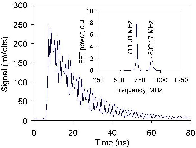
The sample surface is struck by a pulse of laser light, causing it to oscillate at a frequency which is characteristic of the sample material’s properties. A second laser on the inspection system observes the resulting oscillation. The collected data is compared to known properties of the sample material being measured (the particular layer in the wafer’s film stack). Then, parameters such as thickness are extracted and reported by the system while the tool is running; the raw data and calculated parameters are also saved for later analysis.
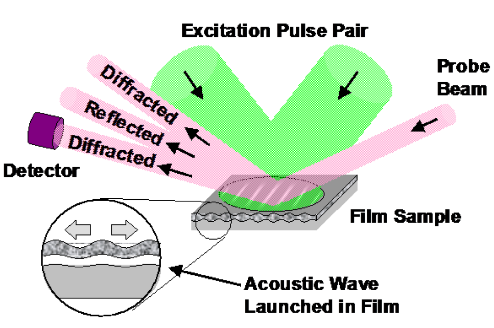
In the SurfaceWave instrument wafers are analyzed one at a time in the measurement chamber. First, an operator or the factory Host requests a specific job to be run. A robot selects the wafer from the carrier (FOUP/SMIF) loaded on the front of the tool, aligns it on the pre-aligner, and places it on the stage in the measurement chamber. Individual sites on the wafer are measured according to the instructions provided in the job’s recipe. When processing is finished, the wafer is removed from the stage and returned to the carrier. Processing continues on the remaining wafers in the carrier until the job is complete. All measurement data is displayed on screen, providing operators with immediate insight into the wafer being processed.
FEATURES
- Fast, non-desctructive measurement method
- Opto-acoustic technique
- Special measurement chamber for wafer analyzing
Product Line
SAW
The SAW product line delivers high-throughput, non-contact, non-destructive measurements of the thickness and uniformity of metal line arrays and pads for all copper/low-k processes. The 3300 is capable of incredible speed and accuracy at the 65 nm node and lower for maximum scalability and the lowest cost of ownership in its class.