


Application
THIN FILM OPTICAL CHARACTERIZATION (R&D)
Thin films can be characterized from different aspects. The below listed applications can provide simple and clear information about the wide range of thin film classification.
- Optical, electronic and energy applications: solar cell materials, thermochromic and electrochromic materials, nanocrystalline films. Thin films and doped layers. Study of temperature-dependent optical phase transitions.
- Bio-ellipsometry: biosensor based on measuring the phase shift and Mueller matrix of monomolecular coatings. Anisotropic materials inspired by nature. Total internal reflection ellipsometry. Study of solid-liquid interfaces.
- Real-time ellipsometry: measurement in situ during vacuum chamber deposition cycles.
- Graphene and novel 2D and 3D materials. Characterization of plasmonic response of patterned surfaces. Specular, and oblique angle scatterometry.
- High accuracy determination of optical functions (refractive index, absorption) versus wavelength.
Technology
SPECTROSCOPIC ELLIPSOMETRY
In the semiconductor industry, there is continuous demand for higher performance and denser integrated circuits. These requirements push the advancement of technology which requires solving of manufacturing challenges. A key to success is to understand the chemical, mechanical and physical properties of wide range of materials used in a typical integrated circuit.
The SE instrument is a combined ellipsometry metrology system with measurement capabilities from the mid-IR to the UV range, which is unique on the market, and is a good candidate for industrial scale metrology solution to determine layer thickness, as well as optical and electrical properties of thin film layers in a non-destructive way.
Spectroscopic Ellipsometry (SE) is a non-destructive optical measurement technique used to determine the thickness and optical properties of thin films and multilayer structures. Ellipsometry measures the phase of the reflected light from the sample, making it relatively insensitive to intensity fluctuations. The raw measurement data represents the complex information from the layer stack, which then needs to be modeled optically. The measurement results are obtained through a numerical regression process of the model data to the raw measurement spectrum.
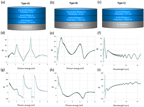
Measurement example on atomic layer deposited, aluminum (Al) doped ZnO (AZO) layers, showcasing the examples of regression:
FEATURES
- Non-destructive optical technique, based on measurement of the change of the polarisation state of light after reflection at non normal incidence on the surface to study.
- It is a higly sensitive even for layer thickness below 5 nm
- Extremely versatile technique: it gives acccess to numerous parameters which characterize multilayer structures (eg. layer thickness, refractive index, absorption, porosity).
Product Line
SE
Refractive optical design in compact realization: short optical path inside the measurement arms (reduced alignment artifact errors). Active temperature control: stabilized environment for system reli-ability enhancement. Uniqe patented high brightness light source for outstanding SNR. CCD detector array (spectrum is taken simultaneously at different wavelengths).
Products

PS-2000, PS-2500
Semilab Porosimeter Series (PS) metrology systems use Ellipsometry Porosimetry (EP) technique to provide reliable and precise measurements of thickness, refractive index, porosity, pore size distribution and Young modulus of porous thin films such as ultra-low K, porous Silicon, nanoparticle layers, metal oxides or barrier layers integrity... Combining solvent adsorption experiments in a high vacuum chamber to Semilab Spectroscopic Ellipsometry (SE) technology, the PS systems form a comprehensive metrology solution, helping our customers to develop, qualify and monitor current and future processes and especially solve the integration challenges of porous low K materials.
The PS Product Family presents various degrees of automation and wafer size capabilities from coupons to 450mm wafers. Its unique technology enables the structural characterization of CVD and spin coated porous thin film without sample scratching or preparation.
An optional heated chamber, available on 300mm selected models, provides advanced measurement capability such as film annealing or Uniaxial Coefficient of Thermal Expansion (CTE), helping chipmakers identify process issues that can lead to film collapse or cracks.
In our fully automated PS-2500 model, a preheating / cooling station allows desorption of residues or organic materials and moisture from the pore before / after measurement, making sure the total accessible porosity is measured and that no solvent remains in the pores if further processing is needed.
Configurations:
| Sample size | Name | Mapping | Features |
|---|---|---|---|
| Up to 300 mm | PS-2000 | Yes | Manual loading automated transfer Optional Heated chamber for CTE measurements |
| 300mm | PS-2500 | Yes |
Fully automated, 1 load port (300 mm) |
Dual load port with OHT available with PS-3000.
Please contact us for 450 mm wafer capable platforms.
PS instruments can also be used to qualify the sealing layer of both patterned and blanket wafers: the instrument detects the diffusion of solvent through the sealing layer, which leads to a change in refractive index measured by Spectroscopic Ellipsometry. Finally, any PS product is also a traditional spectroscopic ellipsometer, which can address characterization needs of non-porous thin films.
Ellipsometry porosimetry (EP) technology was patented by IMEC and licenced exclusively to Semilab.
Request Info

EPA or Vacuum Porosimetry extension for SE-2000 Spectroscopic Ellipsometer
The EPA (Ellipsometric Porosimeter Atmospheric pressure) is designed to allow fast film characterization at ambient pressure and temperature. To make mesopore size investigation simple, cheap, and non toxic, we performed EP measurements using a pulsed air flow with controlled partial pressure of water. This system allows a fast partial pressure equilibration at each point of the isotherm (a complete adsorption-desorption cycle can be obtained within 30 min time)
The EPA setup is made of a spectroscopic ellipsometer on which is fixed a cell of environment control containing the film to analyze. In laboratories, gas volumetry analyses are usually time-consuming, mainly because of long pressure equilibration time within the analysis chamber. In the experimental setup of these experiments, we replaced the pressure equilibration system by a continuous flux of air containing a fixed partial pressure of adsorbate directly in contact with the mesoporous film to analyze.
EPA gives access to:
- Pore size Distribution from 1.5nm to 60 nm diam
- Average pore size
- Porosity
- Cumulative surface area
- Thickness – refractive index – absorption coefficients
- Young Modulus

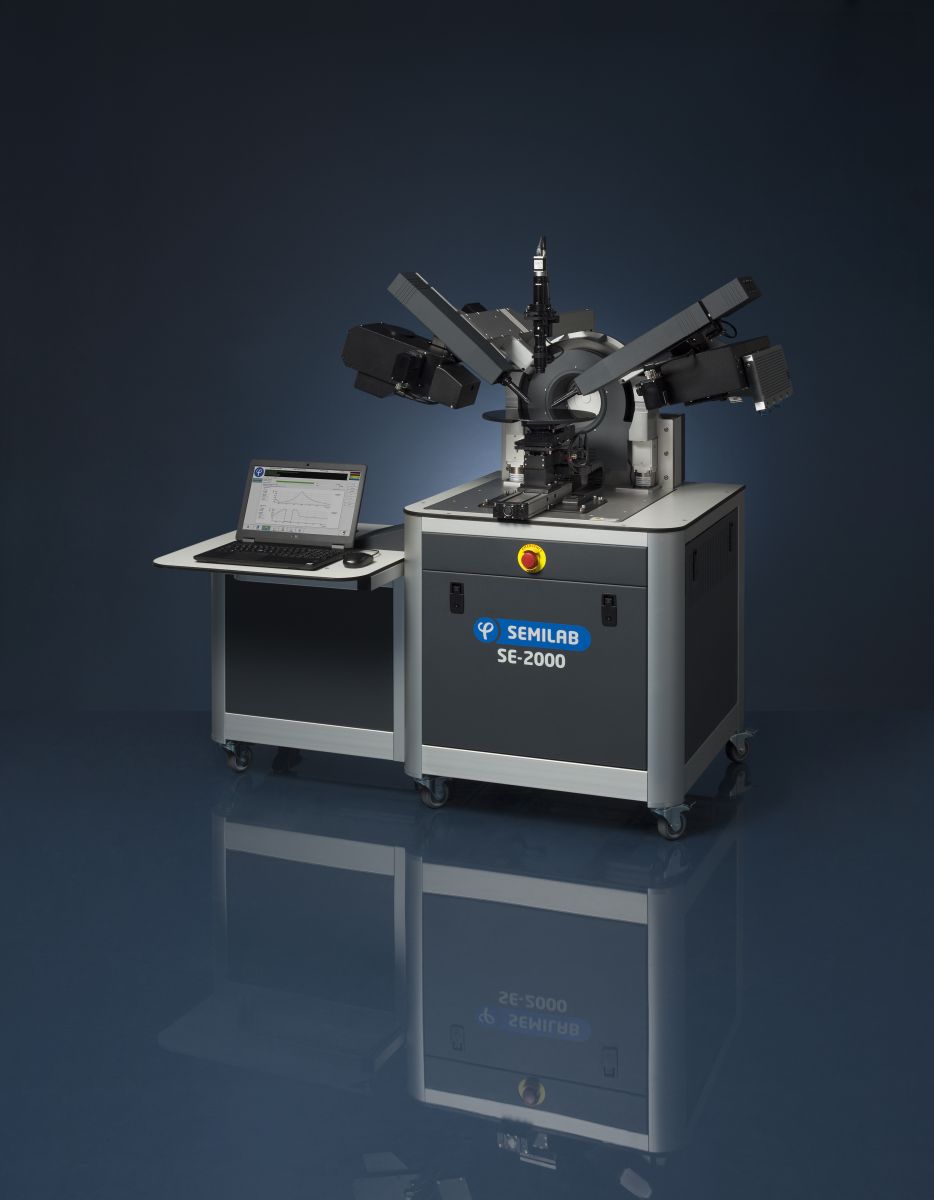
SE-2000 Spectroscopic Ellipsometer
SE-2000 features the widest spectral range available on a single tool. The ranging is from the deep UV (190 nm) up to mid-IR (25 μm). The tool is uniquely offered with an optional FTIR ellipsometer head on the same goniometer with the visible arms. It can be configured with the fast detection mode by using spectrograph and detector array, with the high resolution mode by using spectrometer and single point detectors, or with both modes together on the same tool. SE-2000 includes Semilab’s new smart electronics with interchangeable components, and operates with the new generation operating and analysis software (SAM / SEA). The system can be controlled from a PC or laptop through LAN network, or by a new touch panel interface.
Measurement modes:
- Spectroscopic Ellipsometry for thin film thickness and optical functions, including complex multilayer structures
- Generalized Ellipsometry for anisotropic materials
- Transmission Ellipsometry for transparent substrates
- Scatterometry vs. wavelength and angle of incidence
- Mueller Matrix (11 or 16 elements) uniquely offered in combination with Scatterometry for 3D anisotropic materials
- Jones Matrix for simple anisotropic materials
- Reflectance & Transmittance vs. wavelength and incidence angle
- Polarimetry
- Porosimetry: Measurements of pore size and porosity in thin films
- In situ measurement mode for real time control during deposition or etch process
Options:
- Mapping stage (X, Y, Z, rotation), manual or automatic
- Microspot (standard and ultra small - customization is subject to discussion)
- Environmental cells: cryostat, liquid cell, cooling and heating sample stage cells, QCM cell
- Atmospheric porosimetry chamber
- Visualization camera
- Spectroscopic Reflectometer
- Extended spectral range detection
- Possibility of integration of other Semilab metrologies (4pp, Eddy, etc.)
Request Info

SE-1000 Spectroscopic Ellipsometer - Tabletop Manual System
SE-1000 provides modularity and high measurement performance in a compact table top footprint. This cost-efficient tool includes manual goniometer and manual sample positioning suitable for R&D laboratories. It performs non-contact and non-destructive optical measurements on substrates, single layer and multi-layer samples to obtain individual thin film thickness and optical properties. SE-1000 includes Semilab’s new smart electronics with interchangeable components, and operates with the new generation operating and analysis software (SAM / SEA). The system can be controlled from a PC or laptop through LAN network, or by a new touch panel interface.
Measurement modes:
- Spectroscopic Ellipsometry with rotating compensator
- Generalized Ellipsometry for anisotropic samples
- Mueller matrix 11 coefficients
- Jones matrix
- Porosimetry: Measurements of pore size distribution and porosity in thin films
- In situ measurement mode for real time control during deposition or etch process
Options:
- Microspot
- Near-infrared spectral extension
- Atmospheric thin film Porosimetry
- Liquid cell cooling and heating stages
- Visualization camera
- Spectroscopic reflectometer
- Liquid cell, cooling and heating stages
Request Info


inSE-1000 In-Situ Spectroscopic Ellipsometer
The new in-situ thickness measurement system, inSE-1000 provides instant access to layer thicknesses and optical properties through ellipsometric specra analysis during layer deposition processes in vacuum chambers and load locks.
inSE-1000 is the part of Semilab's ellipsometry tool family specially designed for the measurement on vacuum chambers during deposition or treatment processes or in load locks. The easily mountable arms can be placed on the vacuum chamber or on an offline testbench for detailed investigation of the final product. The electronic components and supplementary systems are situated in a cabinet, which can be placed next to the deposition tool. The ethernet interface allows on-demand measurement sequence with the deposition tool and the two-way communication protocol.
Features and system specifications:
- CF-40 vacuum port interface
- 75 W, short arc Xenon lamp by optical fiber
- Rotating compensator optics
- Beam divergence < 0.2o ( in parallel beam, no focusing)
- Compact arms
- Spectral resolution for fast mode
Software:
- Immediate visualization of the measurement data and the fitting results: thickness and optical properties
- Modelling of each layer with all known methods including dispersion laws, alloy model, periodic layers, phase node model, anisotropic layer evaluation, or user-defined free formula
- Ethernet-based communication protocol with the deposition tool computer
- The largest (n, k) database
Request Info
")
SE-2000-IR Spectroscopic Ellipsometer (IR)
SE is traditionally used in the UV/visible/near-infrared wavelength region (190-2500 nm) for precision metrology of layer thicknesses, refractive indices and alloy concentrations. Semilab proposed a Fourier Transform Infrared Spectroscopic Ellipsometer (SE-2000-IR) for research and development. Infrared region is interesting, because in many cases absorption bounds related to the chemical composition of the sample can be detected. Thickness information can also be gained from the infrared region from interference fringes as in the UV-visible region. Moreover, free carrier concentration affects the absorption coefficient in the infrared range giving a non-destructive way to measure this parameter using the Drude tail.
Request Info
SE-2100
Printed Electronics. Optical & Electrical Metrology. Thin Film Coating characterization. Layer Thickness control.
Features and System specification:
- Capable for Fast and accurate measurement on square samples up to 350x450 mm or wafers up to 300 mm
- Special design of the chuck to hold Flexible Sample
- Active Vibration damping
- High-resolution mapping stage
- Fast Omron autofocus
- Vertical camera for samples visualisation & Pattern recognition
- Joystick to move the sample easily
- CE and SEMI standards compliant
Components & Options:
- Spectroscopic Ellipsometer:
- Fast acquisition directly on the foil
- Measurement Spot adapted for Plastic substrate
- Spectroscopic Reflectometer:
- For reflection and transmission of the films
- Non-contact Sheet resistance:
- Fast and accurate Sheet resistance by Eddy Current
- For Transparent electrode and Metal
- Other measurement technique like Raman, Lifetime...etc
Applications:
- Display: TFT, OLED on Glass or Flexible substrate
- Lighting: New OLED Lighting application. White OLED
- Printed Electronics: Any process on flexible substrate (transistor, sensors, etc.)
- Photovoltaics: Small Thin Films PV panels, TCO panels