


Enhanced Vision – Enhanced Defect Detection
04.27.2023

Explore the Semilab En-Vision system's unique capabilities, applications, and benefits.
En-Vision is a non-contact and non-destructive measurement system that specifically targets quick and precise detection of nm scale buried defects, located under the silicon surface, invisible to conventional inspection tools, impacting device performance and yield. One of the significant advantages of the En-Vision system is its enhanced vision, that allows for advanced defect detection. En-Vision provides unmatched measurement image quality, making defect detection easier and more accurate, and with this, taking defect detection to the next level in all its versatile application possibilities.
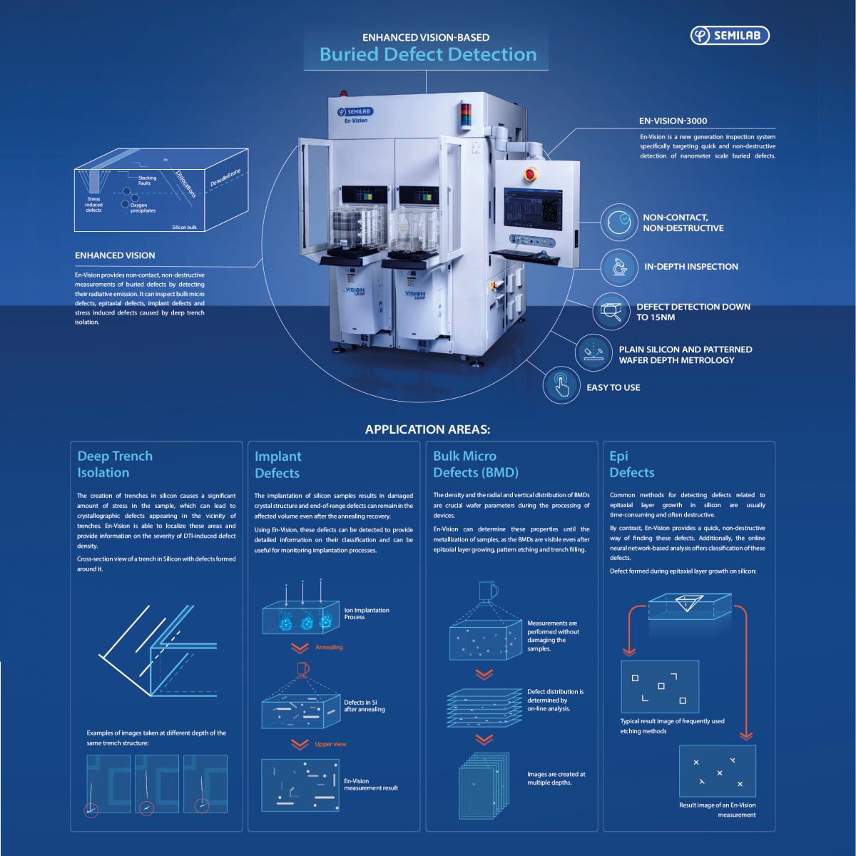
The En-Vision system can help monitor the implantation processes, detect defects in epitaxial layer growth in silicon, and localize crystallographic defects in the vicinity of trenches.
During the implantation process of silicon samples, the crystal structures can be damaged and end-of-range defects can remain in the affected volume even after the annealing recovery. With En-Vision, the implantation processes can be monitored to detect these defects and provide detailed information on their classification. With En-Vision system, bulk micro defects (BMDs) can be detected with detailed information on their density and radial and vertical distribution.
En-Vision is an excellent solution for EPI defect monitoring as well, since traditional methods of detecting defects in epitaxial layer growth in silicon are often time-consuming and destructive. However, En-Vision offers an efficient non-contact and non-destructive method of quickly and cost-effectively identifying these defects.
En-Vision also provides information on the severity of DTI-induced defect density by monitoring the material at different depths and with that it can help detect defects in deep trench isolation and provide material structure characterization.
With its unique capabilities En-Vision allows for more accurate and efficient defect detection through a wide range of applications, whether it's detecting implant defects, bulk micro defects (BMDs), epi defects, or deep trench isolation. This makes En-Vision metrology system a game-changer in the semiconductor industry.
If you want to know more about the Semilab En-Vision system and its results, you can dig deeper in the following publications:
Review of applications of Defect Photoluminescence Imaging (DPLI) during IC processing