


Semilab publishes paper on Lateral mapping of damage patterns in plasma immersion ion-implanted silicon
01.03.2023
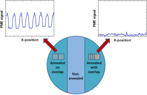
For fine structure shallow junctions formed by plasma immersion ion implantation (PIII), post-implantation annealing can be performed by energetic short laser pulses following a predetermined laser exposure pattern. In this work, 2 kV BF3 PIII has been performed in the dose range 5e14-1e16 cm−2 on p-type (100) Si wafers. PIII was followed by pulsed laser annealing (PLA) applied in both overlapping and non-overlapping laser spot exposure configuration and with different laser energy fluences in the range 0.4–0.6 J cm−2. The effect of both PIII and PLA has been analyzed by photo-modulated reflectance, micro-photoluminescence (μ-PL), and spectroscopic ellipsometry. Wafer-scale maps and line scans clearly show the effect of the laser patterning configuration on annealing. We show that the combination of the applied characterization methods provides effective manufacturing process control and gives valuable information on defect levels, damaged layer thickness, and carrier recombination processes.
The publication, presented by our colleague, Zsolt Zolnai at the International Conference on Ion Implantation Technology 2022 (IIT 2022) in San Diego, is now available to read at MRS Advances.