Application
Technology
INFRARED CONFOCAL MICROSCOPY
Infrared Confocal Microscopy is an excellent tool for crystal investigation without any damage, with a detection limit proven down to 30 nm defect size. Due to the non-destructive nature of the method, pattern recognition features, and precision X-Y mapping stage measurements can be performed at any point of the wafer. Depth scanning of defects is also available.
The detected signal is evaluated by an advanced analysis software, which includes the automatic defect finding algorithm, background correction and scattering exclusion. From the acquired data, a database-friendly file can be generated, which contains all settings and evaluation results.
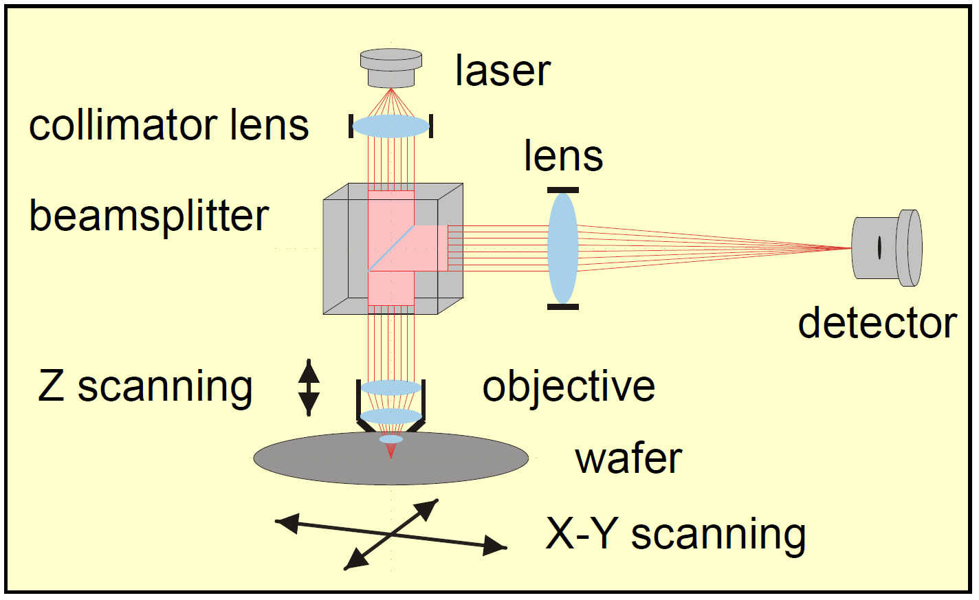 Figure 2. Measurement theory
INFRARED CONFOCAL MICROSCOPY CAN BE IDEAL FOR FINDING THE FOLLOWING DEFECTS:
- Stacking faults in epi layer and in bulk silicon
- Slip lines
- Particles
- Dislocations (for example on oxygen precipitate)
Next to the defect identification, the SIRM product line is capable of measuring the depth profile of BMD density with denuded zone, due to the possibility of setting the distance between the sample surface and the objective.
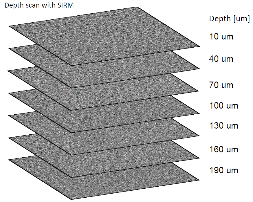 Figure 3. Depth scanning in SIRM
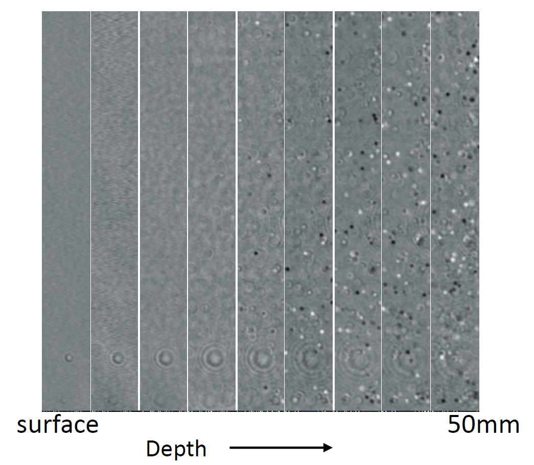 Figure 4. Slip lines
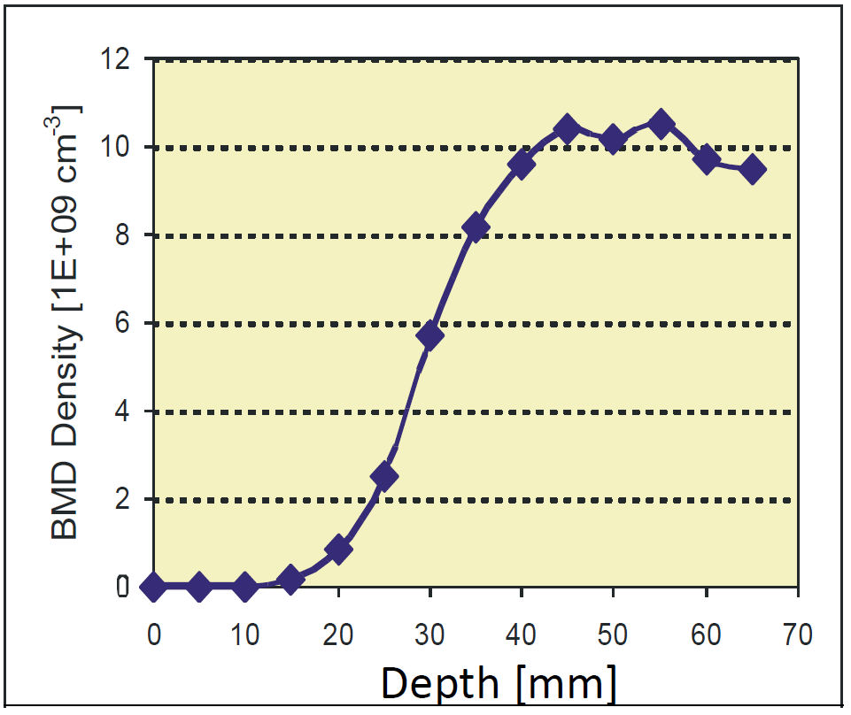 Figure 5. BMD density results
FEATURES
- Non-contact, non-destructive analysis
- No sample preparation is needed
- Image collection in X-Y and X-Z planes
- Insensitive to back surface condition
- Measurement of highly doped epi wafers (epi substrate down to 3 mΩcm)
- Laser marking option
Product Line
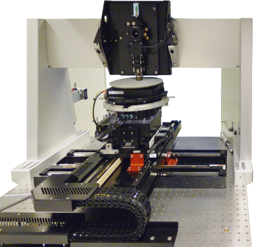
SIRM
The Bulk Microdefect Microanalyzer is a non-contact, non-destructive optical instrument, which provides a complete characterization of bulk microdefects (BMDs), such as oxygen and metal precipitates, voids, stacking faults, slip lines, dislocations in the bulk and in the near-surface region of the semiconductor wafers.
The infrared confocal microscopy technology ensures the precise and fast identification of the defect amounts in much more trustful way, than the manual counting. It is applicable for the depth of 10 μm and higher.