


Application
EPI RESISTIVITY MEASUREMENT
A blanket layer of silicon can be added to a silicon substrate by a CVD process to achieve changes in the properties, like resistivity, type and defect density. This CVD process is called epi (or epitaxial) deposition. The thickness monitoring of the epi layer is part of the production process of making the epi wafers. This monitoring is executed on a sample basis, or only to confirm that the epi reactor is set up properly.
Semilab can offer non-contact optical solution for Epi thickness monitoring, depending on infrared reflection techniques.
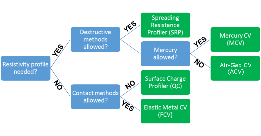 Figure 1. Resistivity measurement flow
Technology
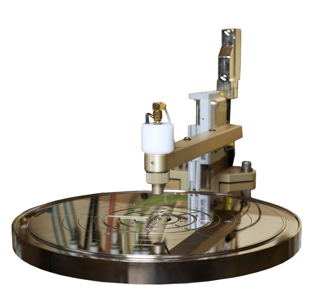
MERCURY CV PROFILING
The MCV systems allow the elimination of the need for costly metal and poly deposition processes by using a pneumatically controlled, non-damaging contact probe design. The system features an extremely stable contact area and uses only a small quantity of mercury to make highly repeatable CV and IV measurements for process development and process monitoring applications. MCV is a superior technique for both bulk/epitaxial- and dielectric layer characterization.
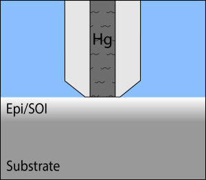 Figure 2. MCV profiling
Modern device structures require accurate and precise resistivity control and carrier density profile of epitaxial silicon. Semilab’s mercury (Hg) Schottky-CV technique is suitable for either production or R&D monitoring, offering speed, high repeatability and sensitivity.
The Hg Schottky-CV technique uses a high repeatability, non-scrubbing, vertical arm probe. The probe includes a 2 cm long capillary that holds a small volume of mercury and is electrostatically shielded to reduce stray capacitance and it’s positional dependence. The epitaxial wafer is placed on the stage, processed side up, either manually or with a robot. The Hg probe is then lowered from the topside in a controlled manner to form a high quality Schottky contact.
The Hg Schottky-CV technique can be used to measure n/n+, p/p+, n/p and p/n epitaxial structures. The carrier density profiles on other semiconductor materials, such as GaAs, GaP, InP and SiC can also be measured.
Examples of the carrier density profiles measured on thin p/p+ epitaxial structures are shown on Figure 3-4.
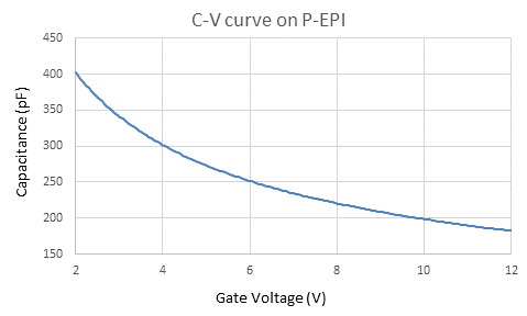
Figure 3. Carrier density profiles on thin p/p+ epitaxial structures
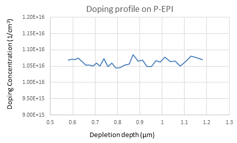
Figure 4. Carrier density profiles on thin p/p+ epitaxial structures
Application and specs |
Measured parameters |
Epitaxial resistivity monitoringDoping range:
Depth and doping ranges limited by zero-bias depletion width, breakdown voltage. Resistivity range for silicon: according to ASTM 1392
|
|
Alternate semiconductor materials
|
GaN:
SiC:
|
The MCV product line also has powerful features for the Electrical Characterization of Dielectrics and Compound Material Characterization.
FEATURES
- Semilab’s mercury (Hg) Schottky-CV technique is suitable for either production or R&D monitoring, offering speed, high repeatability and sensitivity.
- Complete Schottky-CV resistivity profiling for epitaxial layers
- Complete MOS CV electrical characterization for dielectrics to determine thickness, k-value and more
- Advanced CV evaluation for compound semiconductors and special applications (for example HEMT structures) for detailed analysis of semiconductor-dielectric interface parameters
Product Line
MCV
All Semilab's MCV systems are equipped with automated, full hand-off, mercury handling system to increase safety and reliability. The user friendly software environment controls the measurements and also offers a great flexibility for detailed analysis of the measured structures. Full map capability up to 12"/300 mm. All features listed, including optional ones, are compatible with both the manual MCV-530(L) and the automatic
MCV-2200/2500/3000/3000P systems.
On top of the standard CV measurements and standard electronic units, a number of advanced metrology options are available to extend measurement capabilities:
- Multi-frequency CV meter (1kHz to 10MHz), KEITHLEY-4200 for advanced dielectric layer characterization
- Different capillary diameters to meet application demands: standard capillaries d=1.7mm or capillaries with 0.5, 0.7, 1.0 and 4.0mm optionally
- IV option: Current-Voltage based Dielectric Integrity and Reliability investigations
- Pulsed CV option
- Mercury Vapour Analyzer option
Products

MCV-2200, MCV-2500, MCV-3000, MCV-3000P
The MCV automatic mapping systems provide a Mercury C-V measurement for non-patterned wafers used in epitaxial silicon production and front-end semiconductor processing.
In MCV-2200, MCV-2500 and MCV-3000/3000P the wafers are robotically loaded onto the mapping stage from an open cassette or FOUP. The test wafer moves to each site specified in a pre-programmed map as electrical characterization tests are made. The system stores test data and reports them in a variety of formats.
Optional features:
- ID reader (front or back, even in case of transparent samples like SiC, GaN)
- SECS/GEM host communication
- Pre-treatment chamber option
- Can be configured with 300 mm FOUP, 200 mm SMIF or open cassette
Wafer sizes:
- Automatic wafer handling:
- MCV-2200: from 100 mm to 200 mm
- MCV-2500: from 200 mm to 300 mm
- MCV-3000/3000P: 200 mm or 300 mm
- Manual wafer handling:
- Full wafers:
- MCV-2200: from 50 mm to 200 mm
- MCV-2500: from 50 mm to 300 mm
- Coupon samples or fractions:
- minimum sample size is 40 mm × 40 mm
- Full wafers:

MCV-530, MCV-530L
The MCV-530 system is designed for the fast and reliable testing of dielectric and epitaxial layers by mercury probe, and it is ideal for R&D or small volume production.
MCV-530/530L systems are manual loading measurement equipments, however they have the same measurement abilities like the automatic MCV-2200/2500 products.
Wafer sizes:
Manual wafer handling:
- Full wafers:
- MCV-530L: from 50 mm to 200 mm
- MCV-530: from 50 mm to 300 mm
- Coupon samples or fractions:
- minimum sample size is 40 mm × 40 mm

MCV-3000S Facedown Mercury C-V Metrology System
Our innovative MCV-3000S system is configured with Semilab’s new self-aligning probe head design allowing more accurate epitaxial layer characterization on a wide variety of materials up to 300 mm sample sizes, less dependence on sample properties and easier overall maintenance for Si wafermakers.
Semilab MCV-3000S metrology system uses a novel measurement technique. As a result of the fully renewed measurement chamber design the system become capable of accurate characterization of samples with insulating or semi-insulating substrates and samples with a P/N junction, in addition to the capabilities of original MCV tools.
The system is designed to adapt perfectly for fully automated wafer handling of samples up to 300 mm diameter and is equipped with dual load ports that support feed-dump wafer flow, making it ideal for high volume front-end semiconductor production process monitoring. The system’s mini environment provides stable measurement conditions.
Applications
Semilab’s Mercury-contact C-V metrology system is a highly advanced and versatile tool designed for accurate and precise doping and resistivity (valid only for Si) profiling of epitaxial layer structures on bare substrates and characterization of dielectric layers and dielectric-semiconductor interfaces.
Key advantages
- Self-aligning probe head resulting in easier overall maintenance
- Extremely stable Hg return contact supporting measurements to be less dependent on substrate properties resulting in improved measurement accuracy
- Improved tool-to-tool matching
- Only a small quantity of Mercury is used to perform higher level of safety
- Capable of measurement of wide variety of materials - including compound semiconductors
Specifications
- Dual mercury top surface contact design, where both the measurement site and the return contact are formed via mercury on the top surface of the sample
- Wafer flipping mechanism (within the measurement chamber)
- Built-in high-precision Mercury Vapour Monitor
- Mini environment with ULPA filter fan unit(s)
- Full factory automation:
- E84 and OHT capabilities
- FOUP compatible Front-End with dual load-ports
- Automated wafer handling for 300 mm (12”) full sheet wafer samples
- Automated wafer handling for 100-200 mm (4” to 12”) full sheet wafer samples, using adapter plate(s)
- Feed-dump wafer flow is supported
- Pre-Aligner is included
- Wafer ID reader (top, bottom, or both)
Options
- Additional high-precision Mercury Vapour Monitor option
- 3 different reference samples
- Alternative third-party C-V meter options, suitable for multi-frequency measurement
- Wafer Preface Treatment Chamber (PTC) for rapid wafer treatment of full sheet wafer samples
- Wafer ID reader options