


Application
COMPOUND MATERIAL CHARACTERIZATION
Compound materials enable the production of advanced, easy-to-use power devices, ultra-high frequency radio devices and more. These emerging products become more and more prevalent in electric or hybrid cars for example, or in power management and distribution devices related to renewable energy sources. For reliable production, composition and defects, dopant concentration, electrical and optical qualities must be regularly monitored. Semilab offers several products for this purpose. Most products are non-contact and non-destructive, and in many cases, they reveal properties directly related to device characteristics or performance.
Technology
NON-CONTACT MOBILITY BY MICROWAVE REFLECTANCE
Device manufacturers have a critical need to measure mobility. Knowing it as a function of position (mapping) allows for optimization of epi reactors to maximize yield.
The Semilab MBM-2201 and LEI-1600 family allow for non-destructive, non-contact measurement. Our proprietary software takes the microwave response and correlates it to conductive components that can be processed by conventional Hall methods. Time-consuming and destructive Hall measurements can be left in the lab.
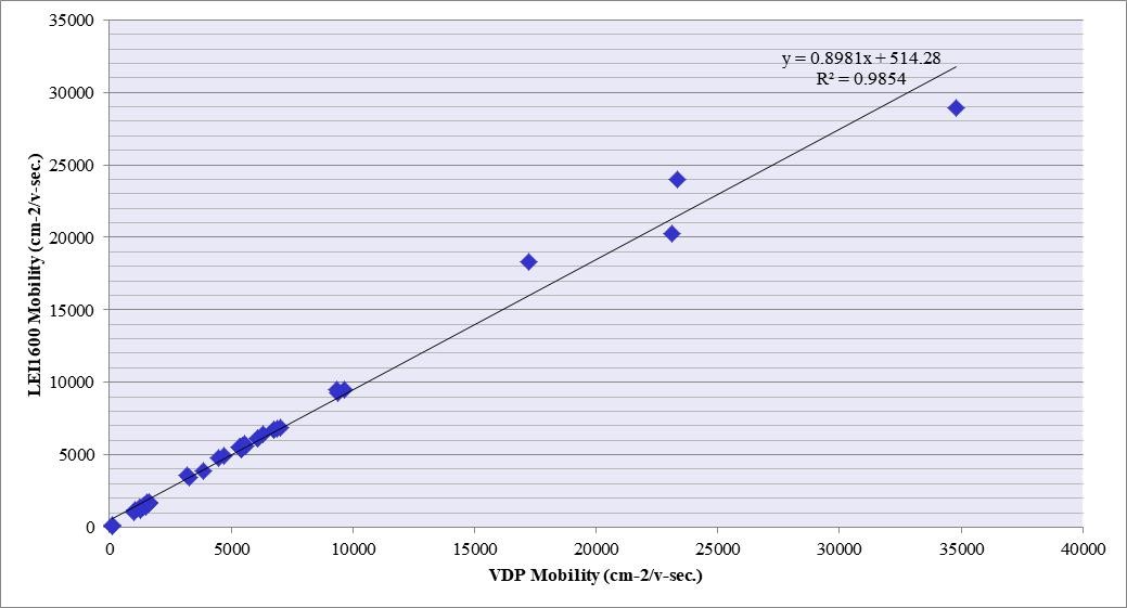 Figure 1. Non-contact mobility measurement compare to destructive process of record
The non-destructive mobility measurement methods of MBM-2201 and LEI-1600 systems can measure various semiconductor transport properties, including mobility, carrier density (sheet or bulk), and sheet resistance via a non-contact measurement method.
The systems use a low-power microwave source operating at 10 GHz, coupled to a waveguide network to direct the power to the surface of the sample under test. The waveguide network allows detection and measurement of both the TE10 and TE11 modes of propagation. The normal TE10 incident wave is used to generate two types of reflected waves returned from the sample under test.
The first wave, the reflected power, is in the same mode (or polarization) as that of the incident wave. The power from this reflected wave is detected, measured and used to calculate the sample’s sheet resistance based on the overall impedance of the waveguide system.
The second wave, the TE11 mode is caused by the "Hall Effect" of the sample under the influence of a magnetic field. The normal TE10 incident wave is rotated 90 degrees by this effect. The system detects and measures the Hall power, then uses this to calculate the remaining transport properties of mobility and sheet carrier density.
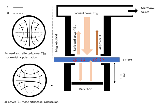
Figure 2. Diagram of the measurement
The non-destructive nature means that mapping can be performed easily.
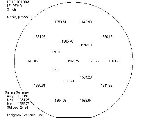
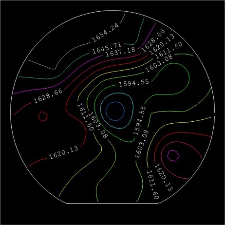
Figure 3. Single field output (carrier mobility)
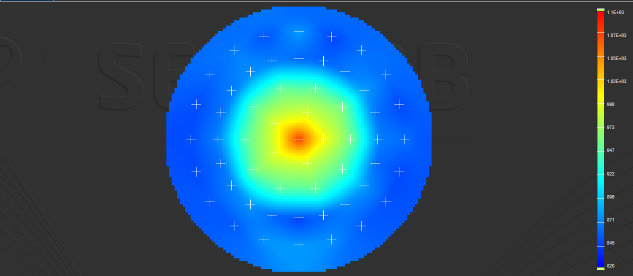
Figure 4. Mobility measurement map: Reference wafer for mapping n-HEMT structure
The value of the microwave mobility is that once the reflected powers are analyzed, they are converted into conductivity coefficients that follow all the rules of standard Hall measurements. They can be processed in the same way and this opens up the way for the same carrier fitting used in conventional Hall.
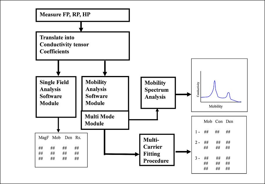
Figure 5. Basic 1610 non-destructive mobility measurement flowchart
In addition, excellent correlation is shown to the conventional technique over multiple technologies.
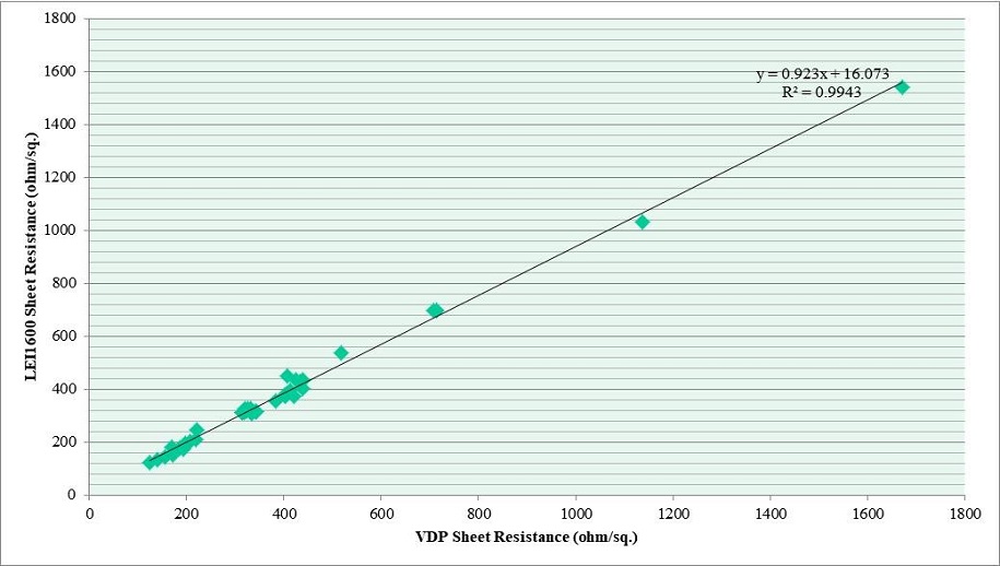
Figure 6. Performance correlation with van der Pauw Hall. Sample include: pHEMT, HEMT structures on CdTe, GaAs, InP, Si, SiC and Sapphire substrates
FEATURES
- Non-destructive measurement method
- No monitor wafers are needed, so test wafers can be sold after measurements
- Eliminates the need for time-consuming sample preparation
- Reduces measurement time from hours to minutes
- Provides instant feedback
- Automated mapping
- Compliant with ASTM F76 Standard Test Methods for Measuring Resistivity and Hall Coefficient and Determining Hall Mobility in Single-Crystal Semiconductors
Product Line
LEI & MBM systems
LEI systems
- Microwave reflectance allows for non-contact mobility measurement
- Ideal for RF device characterization
- Analysis follows conventional Hall methodology for consistency
- Multi-carrier modeling option
MBM systems
- MBM-2201 system with its fully automated measurement method addresses the High Volume Manufacturing market, primarily the RF GaN market
- Microwave reflectance allows for non-contact and non-destructive mobility and sheet resistance measurement
- Ideal for RF device characterization
- Analysis follows conventional Hall methodology for consistency
- SECS/GEM communication capability
Products

LEI-1616AM, LEI-1618AM, LEI-1616RP, LEI-1618RP
The LEI-1616 is ideal for both R&D and volume production of RF devices.
A permanent magnet allows for measurement of mobility as low as 100 cm2/V-s. Sheet resistance of 100-3000+ Ohm/sq is measurable.
The AM is manually loaded and automatically mapped. It accommodates 50-200 mm wafers.
The LEI-1618 adds an integrated eddy current head for improved precision of sheet resistance.
The RP is robotically loaded and accommodates either 50-150 mm or 76-200 mm wafers (option chosen at system build).
Request Info
LEI-1610E100AM, LEI-1610E100R
The LEI-1610E100 is ideal for both R&D and volume production of devices where the mobility is as low as 100 cm2/V-s or multicarrier modeling is of interest.
An electromagnet allows for measurement of mobility as low as 100 cm2/V-s. Sheet resistance of 100-3000+ Ohm/sq is measurable.
The electromagnet also allows for measurements at multiple magnetic (B) fields. This provides an opportunity to model carriers from several layers. This is comparable to the capability of conventional Hall systems.
The AM is manually loaded and automatically mapped. It accommodates 50-200 mm wafers.
The RP is robotically loaded and accommodates either 50-150 mm or 76-200 mm wafers (option chosen at system build).
Request Info
LEI-3200RP
The LEI-3200RP combines the 1610E100 unit with a dedicated sheet resistance unit (1510) to provide the capability to measure sheet resistance from 0.0035 -3000 Ohm/sq. Mobility can be characterized as low as 100 cm2/V-s with multicarrier modeling possible.
Request Info
MBM-2201 Non-Contact Mobility and Sheet Resistance Metrology System
MBM-2201 is the ultimate choice for characterizing the conductive properties of compound semiconductors on the entire sample surface. It provides a non-destructive and non-contact method that characterizes mobility based on RF reflectance and a permanent magnet; and sheet resistance using Eddy Probe measurement of samples up to 200 mm sample sizes.
Improved measurement ranges
- Wide measurement ranges with excellent repeatability
Platform
- Auto-loading of 4"-5" or 6"-8" samples,
- Dual loading station for automatic sample load from open cassettes
- Manual loading of 3” samples
- 200 mm mapping stage
- Designed for ISO Class 1 cleanroom without FFU
- SAM2 based software compliant to SEMI® standard
Options
- SECS/GEM communication capability
- Ionizer
- OCR capability for transparent samples
- Calibration setup wafers