


Application
LABORATORY APPLICATIONS
Troubleshooting manufacturing process needs more comprehensive analysis of the wafers in different process steps. Often these tests are out of scope of in-line and offline process control tools. For this purpose Semilab can offer state-of-the art laboratory tools with multiple capabilities.
These advanced metrology tools can be effectively used in the research and development field to introduce new methods and techniques for high efficiency solar cell production.
Semilab is open for cooperation with customers to improve the tool performance and introduce new applications to cover future metrology needs.
The measurement tools were designed to achieve good tool performance, user-friendly operation and low cost of ownership.
The applications include the following:
- Wafer contamination characterization
- Analytical contamination detection in wafers
- Measurement of electrical parameters in different manufacturing stages
- Optical characterization of deposited layer parameters
- Electrical characterization of deposited dielectric layer parameters
- Measuring surface passivation efficiency and homogeneity
- Testing accelerated light-induced degradation (LID) and potential-induced degradation (PID) of solar cells
Technology
QUASI STEADY STATE -µPCD
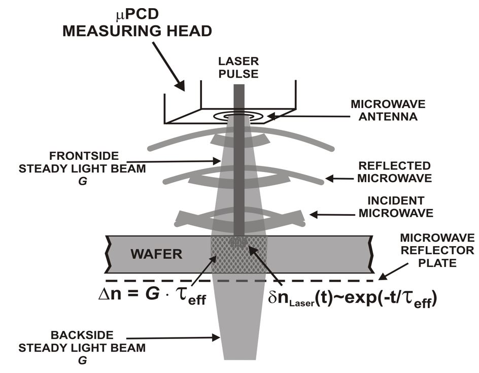
Microwave detected PhotoConductance Decay (µ-PCD) Carrier lifetime measurement is a useful technology for incoming wafer inspection, quality control and process monitoring in wafer manufacturing as well as in solar cell manufacturing. The microwave induced photoconductive decay method is the most common way of measuring minority carrier lifetime in silicon. This method excels due to its reliability, good reproducibility and the short measurement time that permits of making lifetime maps with high resolution.
Frequent contaminants and their lifetime killing efficiency:
|
Level of influence |
Element |
|---|---|
|
Strong |
Fe, Pt, Cu |
|
Medium |
Pd |
|
Weak |
Mo, W |
|
Negligible |
Ca, Al, Zn, Ti |
A contaminant may exist in two molecular states, with different effects on lifetime (or diffusion length).
The change in lifetime, caused by changing the state of the contaminant, measures the amount of that contaminant:
- Requires a unique method of changing states
- Constants are derived empirically
- The effect of a contaminant on lifetime may be dependent on injection level
- Change can be detected by μ-PCD or SPV technique
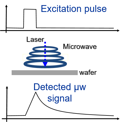
µ-PCD technique
It is a metrology of recombination properties and defects used in silicon photovoltaics and IC manufacturing as well. The technology is based on pulse of laser light, which generates carriers. Excited carriers change the conductivity of semiconductor. The microwave reflection is sensitive to change in conductivity measured signal shows decaying of conductivity. The objective of the monitoring is the bulk lifetime parameter, because that gives information about the contaminations and dislocations.
Role of Crystallinity in case of Multicrystalline Silicon:
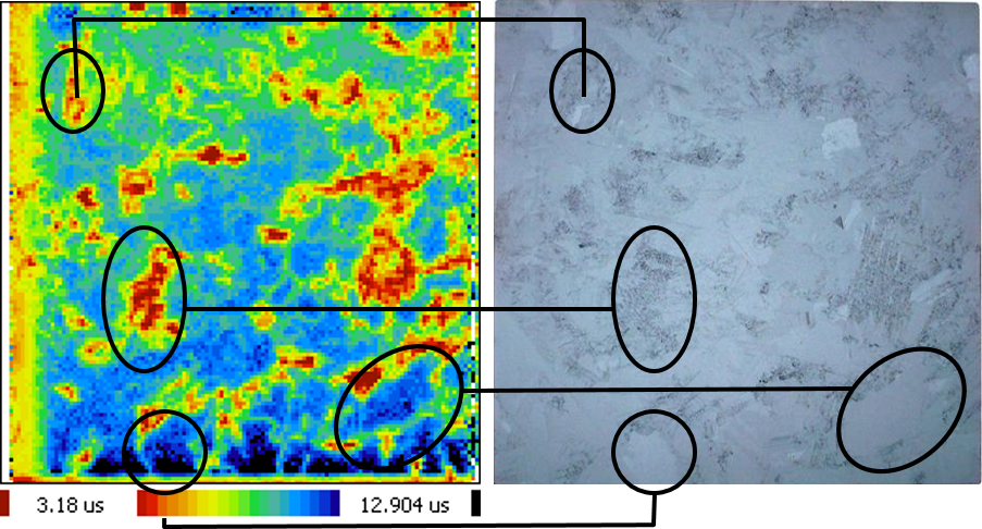 Different lifetime can be observed on different grains
Quasi-Steady-State Microwave detected PhotoConductance Decay
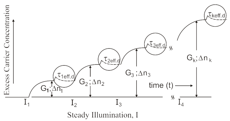
A new powerful version of the technique introduced by Semilab is termed, QSS-μPCD with QDC i.e. the Quasi-Steady-State Microwave (detected) Photoconductance Decay with Quality of Decay Control. It gives enhanced accuracy, new capabilities and broader applications. The technique represents a unified lifetime measurement for silicon PV wafers that enables self-consistent parameter-free determination of two lifetimes most-frequently used in solar cell manufacturing, i.e. the excess carrier decay lifetime, Ʈeff.d, and the quasi-steady-state effective lifetime, Ʈeff.ss. This provides a basis for determination of other recombination parameters important for PV over a broad range of steady-illumination. The technique retains unique wafer mapping advantages of μ-PCD.
In QSS-μPCD technique a decay lifetime measurement is done using a small perturbation transient condition imposed on the steady-state condition. The steady light is turned on to achieve the steady-state condition. Then the short laser pulse generates additional free carriers, and their decay is monitored to determine the decay time constant.
The laser excitation is small compared to steadystate carrier excitation small perturbation condition is well satisfied.
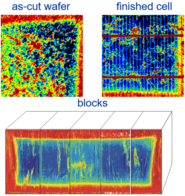
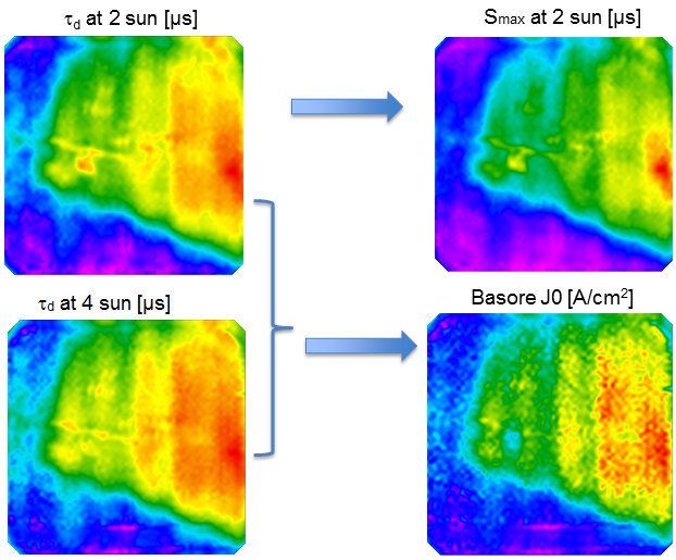
Example of typical QSS-µPCD maps:
FEATURES
- Suitable material to measure:
- Blocks
- As-cut wafers
- Lapped wafers
- Diffused wafers
- Coated wafers
- Finished cells
- Mono-, multicrystalline and EFG material
- Parameter free, non-contact method, suitable for mapping
- Small laser spot diameter
- Suitable material to measure: Passivated surface Si wafers with QSS-µPCD
Product Line
WT, PV
The WT product line is a powerful measurement platform for performing many different semiconductor material characterization measurements. The base system includes all the overhead functions necessary to perform characterization measurements, including power supplies, computer and operating software, XY measurement stage, etc.
The WT-2000 is typically used to make maps, where the wafer is scanned at a programmable raster. Each system is configured to the user’s requirements by adding treatment and measurement capabilities
WT-1200 series are non-contact bulk lifetime and resistivity measurement tools developed specially for mono-crystalline ingots and slugs.
The world’s most powerful PV metrology system. Unparalleled mapping, precision, repeatability and tool matching
Products

WT-1200A
Quasi-Steady-State µ-PCD whit Quality of Decay control (QSS µ-PCD QD). Quality control of wafers and solar cells at different stages of production.
Measured parameters:
- Parameter free determination of Steady State Lifetime and Injection level
- Surface Recombination Velocity (Smax)
- Implied Voc
- Emitter Saturation Current (J0)
Features and System specifications:
- Fully automatic operation and data evaluation
- Measurement selectable at any position on the wafer
- Measurement of mono- and multi-crystalline material
- Patented chemical surface passivation option available for wafers
- Lifetime of wafers can be measured after each process step of solar cell manufacturing:
- Incoming as-cut wafer
- Diffused wafers (with or without phosphorous glass)
- Nitride coated wafers
- Metallized wafers
- Finished solar cells
- Advanced parameters (Smax, Voc, J0) can be measured after surface passivation steps