


Interpreting QD Properties with Deep-Level Transient Spectroscopy
11.16.2023
Quantum dots (QDs) are nanoscale semiconducting crystals with optical and electronic properties that differ from larger particles. Their characteristic feature is the ability to emit light of specific wavelengths when illuminated. This is primarily a size-dependent property, meaning the specific emission wavelength varies by scale. Chemistry and structure play important roles in critical QD properties too, and there is a growing number of QD formulations available (cadmium selenide, lead sulfide, graphene oxide, etc.).
Among the most promising formulations are indium arsenide and gallium arsenide (InAs/GaAs) QDs. These are sometimes called SK QDs, after the Stranski-Krastanov formation process. This self-organising growth method creates a three-dimensional structure when the total deposition of InAs on GaAs substrates reaches a critical thickness. Issues inherent in this process include the lack of control over size and morphology, thus the very properties that make QDs so promising.
Understanding the Value of InAs/GaAS QDs
InAs/GaAs quantum dots are highly promising. Growth via molecular beam epitaxy (MBE) offers greater controllability, enabling greater applicability in optical applications. They play a pivotal role in solid-state quantum technology, enabling significant advancements such as single-photon generation and vacuum Rabi splitting. Their application extends to various quantum devices, such as lasers, optical switches, and quantum dot solar cells, leveraging their high quantum efficiency and broad wavelength tunability. The strong confinement of electronic states, attributed to the lattice mismatch between InAs and GaAs, enhances their electronic and optical characteristics. This makes them ideal for quantum communication technologies, including the generation of entangled photon pairs and single-photon sources
The heart of characterizing these promising QDs lies in the ability to effectively interpret their properties, for which deep-level transient spectroscopy (DLTS) is instrumental. DLTS provides insights into the defects and impurities in semiconductors, which greatly affect their photonic performance. However, interpreting DLTS data from InAs/GaAs QDs presents challenges due to the size variability and multi-particle effects intrinsic to these nanostructures.
Advances in DLTS techniques tailored for quantum dots are helping to overcome these challenges. This has become increasingly important as nanofabrication methods—integral to device integration—affect the optical properties of these nanostructures. For instance, the linewidth broadening effect, indicative of the coherence of emitted photons, can be significantly altered by the epitaxial interface quality and nearby etched sidewalls. Surface treatments, such as atomic layer deposition (ALD), have proven effective in mitigating defects that cause spectral wandering—a phenomenon where the emission wavelength of the QD fluctuates over time.
The precise control of QD characteristics achievable through these methods is crucial, particularly when employing second-order correlation measurements to estimate quantum efficiency—a key performance metric for single-photon sources. This metric is vital for quantum computing and communication applications, where the purity and indistinguishability of single photons are paramount.
Looking for DLTS Solutions?
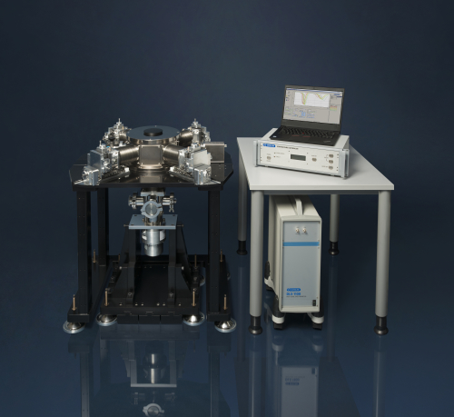
In the pursuit of advancing semiconductor technology, particularly with the promising InAs/GaAs quantum dots, the role of precise characterization tools is paramount. Semilab is at the forefront of this endeavor, offering a suite of solutions for semiconductor analysis, including our state-of-the-art DLTS systems. Our DLTS technology is adept at detecting and characterizing electrically active defects, providing comprehensive insights into trap parameters such as energy levels, capture cross-sections, and concentration distributions. While the technique is inherently destructive, requiring a small sample form factor, the depth of information it yields is invaluable for semiconductor development.
We invite you to explore the capabilities of our DLS-83D, and DLS-1100 DLTS systems, along with our diverse range of cryostats, each tailored to meet specific research and industrial needs. The DLS-1100 system, in particular, is designed for meticulously monitoring and characterizing deep levels caused by defects and impurities, essential for both intact devices and semiconductor materials research. With applications spanning wafer and EPI manufacturers, IC fabs, and research institutes, our DLTS systems are engineered to catalyze innovation and drive the semiconductor industry forward.
Discover how Semilab's solutions can facilitate your research and production needs by visiting our product pages and blogs. Uncover the intricacies of your semiconductor samples with precision and confidence and join us in shaping the future of quantum dot technologies and semiconductor excellence.
References
- Engström, O., Kaniewska, M. Deep Level Transient Spectroscopy in Quantum Dot Characterization. Nanoscale Res Lett 3, 179 (2008). https://doi.org/10.1007/s11671-008-9133-5
- Engström, O., & Kaniewska, M. (2008). Deep Level Transient Spectroscopy in Quantum Dot Characterization. Nanoscale Research Letters, 3, 179 - 185.