


SEMILAB publishes paper about Application of light scattering tomography for Si(111) samples
05.11.2021
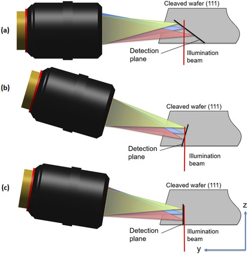 The detection of bulk micro-defects in Czochralski-grown silicon (Si) 〈100〉 wafers has significant importance in wafer quality control. Light Scattering Tomography (LST) is an industry standard technique for this purpose. This optical non-contact metrology requires destructive sample preparation: Samples have to be cleaved into half. One particular feature of the method is a dark field detection arrangement, which is achieved by separating the light detection part (microscope unit) from the illumination. Illumination is applied to the front surface of the sample, and the light scattered off of the defects is collected via the cleaved surface. The technique requires the perpendicularity of the cleaved surface to the front surface, which is fulfilled for Si(100) wafers. However, the nominally cleaved surface for Si(111) wafers is not perpendicular to the front surface but has an angle of 70.5°. This significant difference in cleavage results in the fact that Si(111) wafers cannot be measured by standard LST systems. Fortunately, the standard LST system can be modified by tilting the detection part under a proper angle allowing the measurements of Si(111) samples. In this article, we present this new technique in detail, showing the design and measurement capability of the new system. The measurement results are validated by a direct comparison to standard LST measurements on the same samples after proper sample preparation.
Read more about our research in Review of Scientific Instruments 92, 053701(2021); https://doi.org/10.1063/5.0036868