Application
ION IMPLANT MONITORING
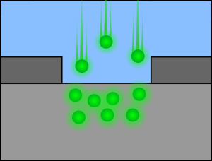
Modern semiconductor devices require precisely controlled dopant concentration and position, and this can be achieved by ion implanting with careful annealing. Typically an n-type species is implanted into a p-type material, or the other way around. Typical species to implant can be boron and indium for the p-type, phosphorus, arsenic and antimony for the n-type layer. Implants are monitored by adding a monitor wafer, and the monitor wafers are checked after the implantation and annealing. Alternatively, the monitoring can be performed by using test boxes on product wafers.


 Figure 1. Implantation