


Application
THIN FILM OPTICAL CHARACTERIZATION (R&D)
Thin films can be characterized from different aspects. The below listed applications can provide simple and clear information about the wide range of thin film classification.
- Optical, electronic and energy applications: solar cell materials, thermochromic and electrochromic materials, nanocrystalline films. Thin films and doped layers. Study of temperature-dependent optical phase transitions.
- Bio-ellipsometry: biosensor based on measuring the phase shift and Mueller matrix of monomolecular coatings. Anisotropic materials inspired by nature. Total internal reflection ellipsometry. Study of solid-liquid interfaces.
- Real-time ellipsometry: measurement in situ during vacuum chamber deposition cycles.
- Graphene and novel 2D and 3D materials. Characterization of plasmonic response of patterned surfaces. Specular, and oblique angle scatterometry.
- High accuracy determination of optical functions (refractive index, absorption) versus wavelength.
Technology
SPECTROSCOPIC REFLECTOMETRY
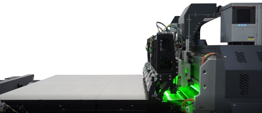
Spectroscopic Reflectometry is a widely-used tool for thin film characterization. The measurement provides information on film layer thickness and optical properties. Spot size can be as small as 5 µm which allows us to measure inside the sub-pixel, consequently no separate test pad is needed for the measurement.
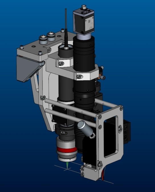
In Semilab SR metrology, wide range of wavelength and high intensity Xe-lamp is used, which makes possible to select the measurement wavelength range according to specific process requirements of the Customer. For thicker layers near-infrared extension can be added which allows to us measure up to several tens of micrometers. An UV-filter can also be added to protect the photoresist or other sensitive layers from UV-light. Due to the large light intensity, acquisition time can be reduced to several milliseconds. Fast focusing and precise movement can be performed due to the integrated laser optical displacement sensor and the 2D camera.
Spectroscopic Reflectometry and Ellipsometry both use the same analysis engine. Consequently, the same optical model can be used for the same material even if being measured by two different metrologies.
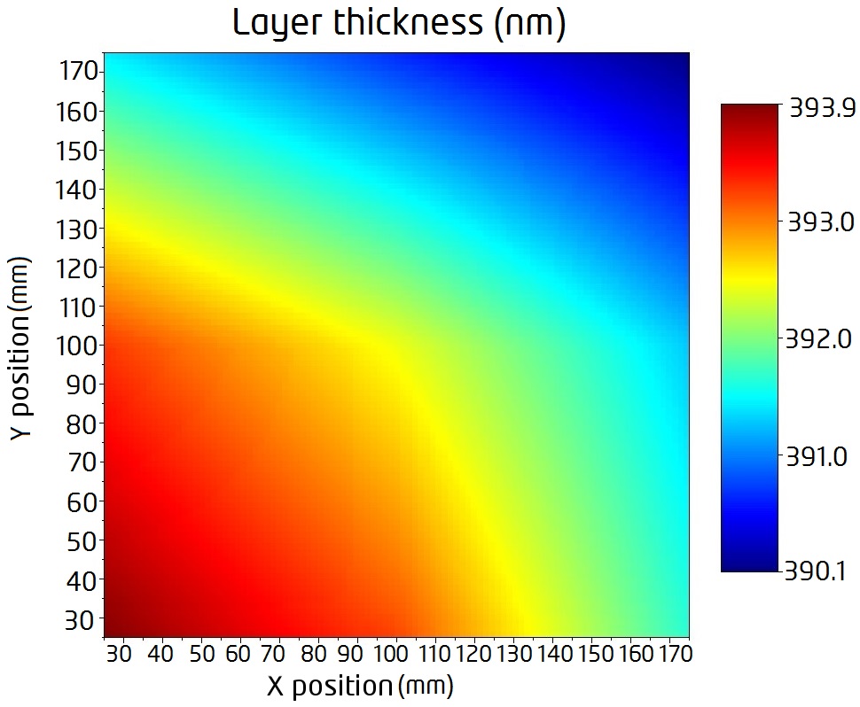 Organic layer thickness map
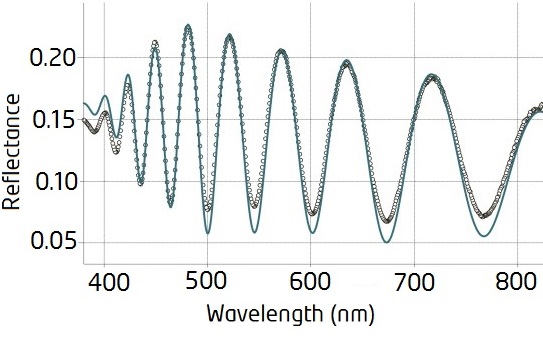
Measured and fitted reflectance curve on an organic layer
FEATURES
- Selectable spot size
- Fast acquisition time
- Easy and straightforward way of optical modeling
- Same optical model can be applied for ellipsometry, reflectometry and Imaging Spectroscopic Reflectometry
- Large wavelength resolution
Product Line
FPT
FPT- series are dedicated for flat panel testing and characterization. The products are designed to characterize LCD and AMOLED TFT panels up to GEN 8.5. It is capable to combine several measurement probes into one platform, providing high precision measurements over the entire surface of flat panels with high accuracy and fast motorization stage and weight capacity.
Products

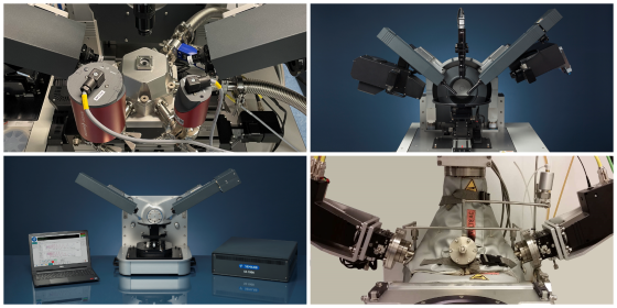
SE-2000 Spectroscopic Ellipsometer
SE-2000 features the widest spectral range available on a single tool. The ranging is from the deep UV (190 nm) up to mid-IR (25 μm). The tool is uniquely offered with an optional FTIR ellipsometer head on the same goniometer with the visible arms. It can be configured with the fast detection mode by using spectrograph and detector array, with the high resolution mode by using spectrometer and single point detectors, or with both modes together on the same tool. SE-2000 includes Semilab’s new smart electronics with interchangeable components, and operates with the new generation operating and analysis software (SAM / SEA). The system can be controlled from a PC or laptop through LAN network, or by a new touch panel interface.
Measurement modes:
- Spectroscopic Ellipsometry for thin film thickness and optical functions, including complex multilayer structures
- Generalized Ellipsometry for anisotropic materials
- Transmission Ellipsometry for transparent substrates
- Scatterometry vs. wavelength and angle of incidence
- Mueller Matrix (11 or 16 elements) uniquely offered in combination with Scatterometry for 3D anisotropic materials
- Jones Matrix for simple anisotropic materials
- Reflectance & Transmittance vs. wavelength and incidence angle
- Polarimetry
- Porosimetry: Measurements of pore size and porosity in thin films
- In situ measurement mode for real time control during deposition or etch process
Options:
- Mapping stage (X, Y, Z, rotation), manual or automatic
- Microspot (standard and ultra small - customization is subject to discussion)
- Environmental cells: cryostat, liquid cell, cooling and heating sample stage cells, QCM cell
- Atmospheric porosimetry chamber
- Visualization camera
- Spectroscopic Reflectometer
- Extended spectral range detection
- Possibility of integration of other Semilab metrologies (4pp, Eddy, etc.)
Request Info