


Application
EPI THICKNESS MEASUREMENT
A blanket layer of silicon can be added to a silicon substrate by a CVD process to achieve changes in the properties, like resistivity, type and defect density. This CVD process is called epi (or epitaxial) deposition. The thickness monitoring of the epi layer is part of the production process of making the epi wafers. This monitoring is executed on a sample basis, or only to confirm that the epi reactor is set up properly.
Semilab can offer non-contact optical solution for Epi thickness monitoring, depending on infrared reflection techniques.
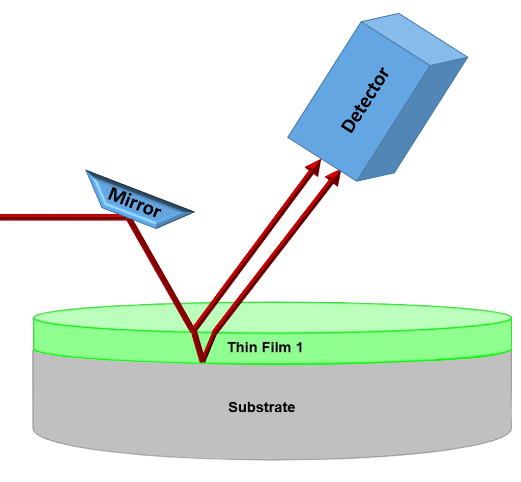 Figure 1. Epi deposition
Technology
FTIR REFLECTOMETRY
Fourier Transformed Infrared Spectroscopy (FTIR) based on Michelson Interferometer is a non-contact, non-destructive measurement technique for EPI thickness, dielectric composition, bulk impurities and high dopant concentration monitoring.
It allows industry standard rapid interferogram measurement for epi thickness, reflection spectrum measurement for multilayer analysis and dielectric composition measurements, and optionally transmission measurement for absorption peak analysis.
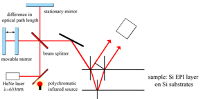
Figure 2. FTIR measurement principles
Interferogram measurement
1. Si EPI Thickness with Interferogram
- Fast and precise measurement
- Thickness information is directly acquired from the two side burst position in the interferogram
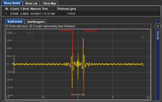
Figure 3. Igram measurement example
Reflection measurement
2. Transition zone thickness acquired from Reflectance measurement using optical modelling
- To acquire more information about the Si EPI sample
- Si EPI can be modelled with an undoped EPI layer, a Doped Substrate, and the transitioning between can be modelled with sublayers of discretely increasing dopant concentration.
- Using Drude dispersion law, modelling is also capable of giving substrate dopant information.
- The goodness of fit parameter can be used to ensure model reliability.
- EIR transition zone thickness results are well correlated with SEMILAB’s Spreading Resistance Profiling (SRP) measurements
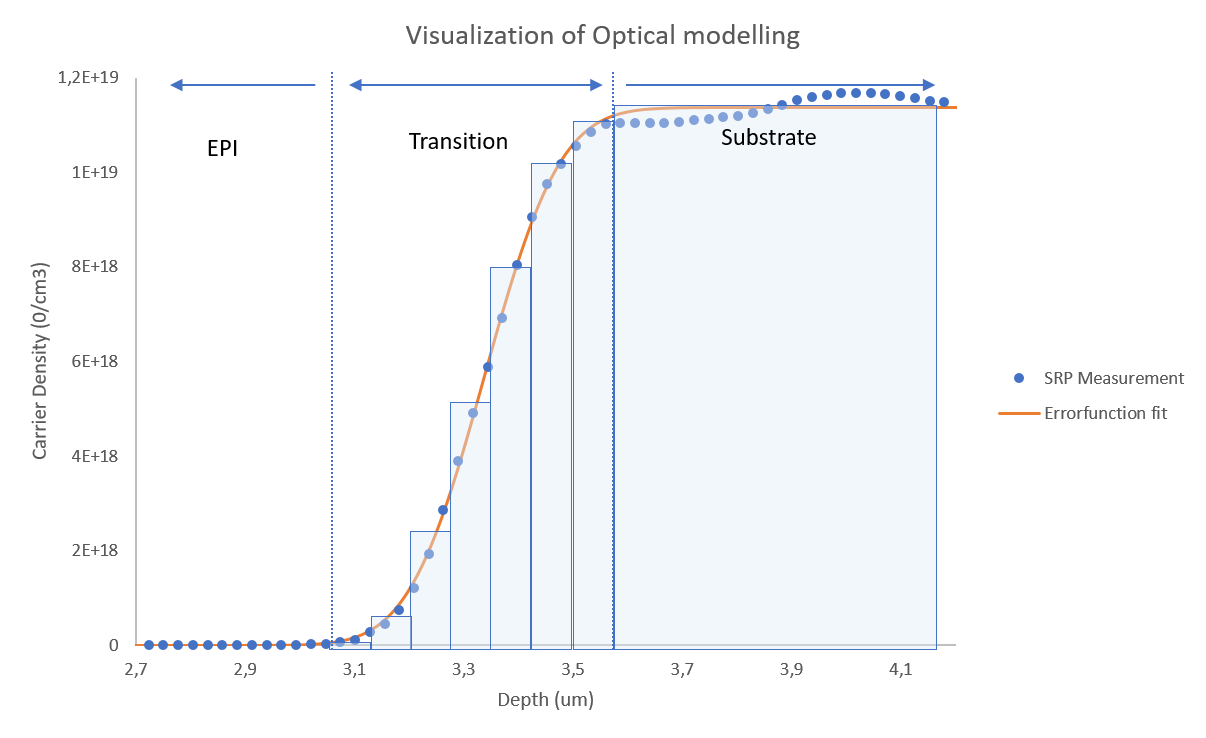
Figure 4. Visualization of optical modelling, using optical model on transmission spectra real time example
3. BPSG concentration measurement using PLS algorithm
- PLS (Partial Least Squares) multivariate calibration is implemented in the Semilab SAM software which is useful for dielectric concentration measurements.
- Using a suitable calibration and validation sample set,the built model can be used to analyze the concentration and thickness of dielectrics similar to the calibration samples in real time.
- This analysis method can be used for more complex peak dependencies such as the case of BPSG.
Transmission measurement
4. Peak analysis in transmission spectra
- Transmission measurement can be used to analyze characteristic absorption peaks of wafers, which are proportional to layer thickness and the bond concentrations.
- Peak analysis can be used to acquire the H concentration in SiN layers by measuring the Si-H and N-H peak heights and area, located at the 2160cm-1 and 3350cm-1 wavenumbers.
- In case of high resistivity Silicon, using a Float Zone Si as reference, with standard ASTM-based calculation the interstitial Oxygen concentration can be also determined from the 1107 cm-1 peak height
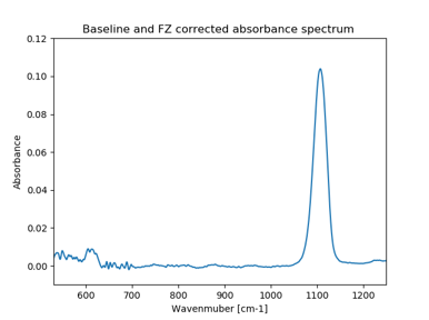
Figure 5. Baseline and FZ corrected absorbance spectrum of Si
FEATURES
The system has a strong modular and versatile design to meet the needs of a high reliability, high throughput epi thickness measurement.
- Applicable for single- and multilayer structures - thickness measurement of each individual layer
- Non-contact and non-destructive optical measurements
- State-of-the-art automation
- Optional measuring method: direct or optical modeling
- Applicable materials: Si, SiC, SOI
Product Line
EIR
- Complex analysis solutoins
- Versatile open modelling software - free recipe creation without limitation
- BPSG monitoring in both reflection and transmission mode
- Accuracy
- Smaller spot size leading to lower Edge Exclusion
- Fast X-Y stage
- Model based measurement with improved accuracy and additional parameter monitoring (EPI thickness, TZ, dopant)
Products

EIR-3000 Enhanced Infrared Reflectometer
The EIR-3000 is a unique automated epi thickness measurement system with infrared spectroscopic reflectometer for high throughput epi thickness measurement. Fully compliant to the relevant SEMI / CE standards. The EIR product line is based on smart, reliable electronics, which improves equipment uptime and decreases maintenance needs.
Applications
- Interferogram measurements:
- Si EPI thickness measurement
- Reflection measurement:
- Si, SiC, SOI thickness measurement of full sheet wafers
- Allows more complex analysis of materials: Transition zone and higher dopant concentration measurement of Si, SiC samples, oxid thickness in SOI samples
- Dielectric composition and thickness measurement: PSG, BSG
Features
| EIR-3000 | |
|---|---|
| Loadport | 1 or 2 loadports, full OHT compatibility |
| Sample sizes | 12” |
| Substrate materials | Si |
| Edge grip | Edge grip robot by default |
| FFU | FFU included |
| SECS/GEM compatible | Yes |
Options
- BPSG and FSG application options
- Transmission measurement option:
- Absorption peak analysis such as Si-H and N-H peak in SiN samples, O-H bonds for water contamination monitoring
- Bulk impurity measurement of Oi
- Signal tower with 4 colors
- Ionizer

EIR-2201 Enhanced Infrared Reflectometer
The EIR-2201 is a unique automated epi thickness measurement system with infrared spectroscopic reflectometer for high throughput epi thickness measurement. Fully compliant to the relevant SEMI / CE standards. The EIR product line is based on smart, reliable electronics, which improves equipment uptime and decreases maintenance needs.
Applications
- Interferogram measurements:
- Si EPI thickness measurement
- Reflection measurement:
- Si, SiC, SOI thickness measurement of full sheet wafers
- Allows more complex analysis of materials: Transition zone and higher dopant concentration measurement of Si, SiC samples, oxid thickness in SOI samples
- Dielectric composition and thickness measurement: PSG, BSG
Features and System Specifications
| EIR-2201 | |
|---|---|
| Loadport | 2 open cassettes |
| Sample sizes | 4-5” or 6-8” |
| Substrate materials | Si, SiC |
| Edge grip | Non-edge grip |
| FFU | without FFU |
Options
- BPSG and FSG application options
- Transmission measurement option:
- Absorption peak analysis such as Si-H and N-H peak in SiN samples, O-H bonds for water contamination monitoring
- Bulk impurity measurement of Oi
- SECS compatibility option
- Signal tower with 4 colors