


Application
COMPOUND MATERIAL CHARACTERIZATION
Compound materials enable the production of advanced, easy-to-use power devices, ultra-high frequency radio devices and more. These emerging products become more and more prevalent in electric or hybrid cars for example, or in power management and distribution devices related to renewable energy sources. For reliable production, composition and defects, dopant concentration, electrical and optical qualities must be regularly monitored. Semilab offers several products for this purpose. Most products are non-contact and non-destructive, and in many cases, they reveal properties directly related to device characteristics or performance.
Technology
RESISTIVITY MEASUREMENT FOR SEMI-INSULATORS
Knowing the uniformity of resistivity and mobility values is critical to achieve process optimization.
A capacitive measurement circuit measures the impedance through an oscillating circuit. Since a capacitor is an effective break in a circuit within a DC environment, charge builds up on the plates of the capacitor, causing a charge imbalance—and then the system stabilizes.
Semilab's COREMA systems are based on a contactless capacitance technique used for precise resistivity characterization of semi-insulating compound semiconductors over a wide resistivity range, useful for the device manufacturing industry.
For the following application fields the main measurable materials are
- Compound Semiconductor (CS) Substrate Resistivity:
- GaAs - RF, Optoelectronics/Photonics
- InP – Optoelectronics/High speed electronics/Photonics, Photovoltaics
- SiC – RF, High power electronics
- Compound Semiconductor (CS) Temperature dependence of Resistivity:
- SiC, GaN, Cd
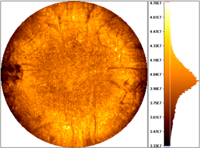
Resistivity topogram of 100 mm GaAs wafer
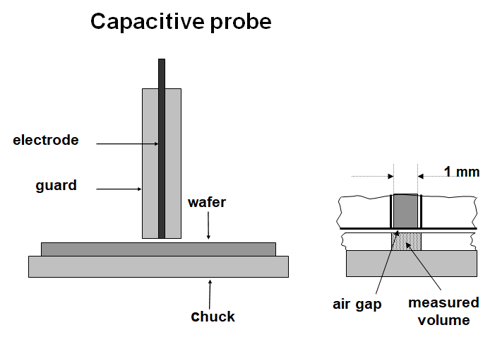 Capacitive measurement method
Principles of resistivity measurement using capacitive probe
- Capacitive metal electrode is positioned above the sample during capacitance-based resistivity measurement. The wafer is moved in XY direction by the stage
FEATURES
- Non-contact, non-destructive measurement method,
thus sample wafers can be sold or put back to production after measurements
- Wide measurement range (1x10⁵-1x10¹² Ωcm)
- No calibration needed
- Fulfills SEMI-M87-0116 standard
Product Line
COREMA
Semilab COREMA systems are capable of
- measuring the following compound semiconductors: GaAs, SiC, GaN, CdTe, InP,
- resistivity measurement of compound semiconductors over a wide range (1x10⁵-1x10¹² Ωcm),
- mapping semi-insulating semiconductor QA processes, as they show inhomogeneities that occur during manufacturing.
Products

COREMA-2000 Contactless Resistivity Mapper
Semilab's COREMA-2000 system is based on a contactless capacitance technique used for precise resistivity characterization of semi-insulating compound semiconductors over a wide resistivity range, useful for the device manufacturing industry.
Knowing the uniformity of resistivity and mobility values is critical to achieve process optimization.
Mapping is critical for semi-insulating semiconductor QA processes as they show inhomogeneities that occur during manufacturing
Application
- Measures compound semiconductors: GaAs, SiC, GaN, CdTe, InP
- Resistivity measurement of compound semiconductors over a wide range (1x10⁵-1x10¹² Ωcm)
Features
- Manual wafer handling up to 200 mm
- Mapping capability
- Colored topogram display of full wafer
- Semi-automatic pneumatic placement
- User-friendly measurement control software
Benefits
- Contactless, non-destructive measurement over the entire wafer surface
- Fast evaluation
- Excellent repeatability
- No calibration necessary