


Application
COMPOUND MATERIAL CHARACTERIZATION
Compound materials enable the production of advanced, easy-to-use power devices, ultra-high frequency radio devices and more. These emerging products become more and more prevalent in electric or hybrid cars for example, or in power management and distribution devices related to renewable energy sources. For reliable production, composition and defects, dopant concentration, electrical and optical qualities must be regularly monitored. Semilab offers several products for this purpose. Most products are non-contact and non-destructive, and in many cases, they reveal properties directly related to device characteristics or performance.
Technology
SPECTRAL PHOTOLUMINESCENCE MEASUREMENT
Spectral photoluminescence (PL) is a non-contact, non-destructive, spectroscopy-based measurement technique to probe the electronic structure of different materials. Spectral PL can be used to obtain information on the emission properties of different heterostructures (quality control) and/or crystal structure of the material.
Photoluminescence is a photon emission process that occurs during relaxation from electronic and/or localized (defects) excited states. Charge carriers can recombine through Shockley-Read-Hall (SRH) and radiative recombination simultaneously. The radiative recombination rate is proportional with the product of electron and hole concentrations. As the minority carrier density is decreased by the SRH recombination that takes place at defects and impurities, the radiative recombination is inversely proportional to defect density and impurity concentration. During radiative recombination, a photon is emitted, which can be detected by a spectrograph. This is the photoluminescence (PL) signal.
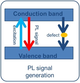 Figure 1. Photoluminescence signals
Semilab offers the spectral PL metrology possibility to characterize compound semiconductors from DUV to NIR spectral region (GaN, SiC, GaAs/InGaAs, GaP). Monitoring of Al-content of AlGaN alloys, PL wavelength dependence as a function of dopant concentration of GaN and GaAs materials, monitoring of single and multi-layer stacking faults of epi SiC layers are covered by our PL metrology tools. Furthermore, the combination of PL and other metrology units (for example Raman, spectral ellipsometry (SE), imaging spectroscopic reflectometry (iSR)) is possible for our medium and big sized platforms allowing the measurement of spectroscopic and thickness data from the same location.
The excitation laser(s) are focused on the sample with a spot size between 10-100 µm. The Semilab PL systems use multiple lasers that are coaxial and have achromatic optics to enable a wide range of applications. The light of the radiative recombination is emitted isotropically inside the sample, which is then collected by spectrographs working either in the visible or the near-infrared ranges. The optical system is designed in such a way that the excitation lasers are highly suppressed, thus the reflected laser light does not disturb the PL signal.
The dual spectrograph setup allows the user to cover a very wide range of samples with PL signal from the UV to the near-infrared spectrum without any need to mechanically reconfigure the system.
Our PL systems are computer-controlled equipments, suitable for recording, storing and displaying photoluminescence maps. Fundamental parameters of the PL spectra like wavelengths, intensities and full width half maximums (FWHM) are analysed in real time.
The Semilab PL systems are equipped with high accuracy detectors, very fast motion stages that enable the recording and analysis of PL maps with extremely high resolution. These maps allow a very precise characterization of the production line performance and provide a rapid feedback for process optimization.
FEATURES
- Quality control and defect monitoring of compound semiconductor samples up to 300 mm
- Non-contact & non-destructive
- Pattern recognition option
- Advanced analysis capabilities enabling real-time inline process monitoring
Semilab SPL metrology solutions combine:
- Spectral photoluminescence,
- Spectroscopic reflectometry (SR) and
- Bow/warp measurement and
- Combo tool option available with macro-spot spectroscopic ellipsometry (SE).
Product Line
SPL
Semilab Spectral Photoluminescence systems can discover several challenges during compound wafer production or EPI layer growth.
- Defect monitoring of wafers used for RF & power devices,
- Epi defect monitoring of SiC, RF & power devices and micro-LED applications,
- Impurities’ detection in GaN, SiC,
- Al-content determination in AlGaN barrier layer
- Composition homogeneity of RF & power device and micro-LED applications,
- Thickness homogeneity (SR) of RF & power device and micro-LED applications,
- Bow/ warp measurement of RF & power device applications.
Products

SPL-2200 & SPL-3000
The reliable SPL-2200 and SPL-3000 systems are designed for diverse inline process monitoring needs with versatile measurement solutions, advanced analysis capabilities enabling real-time quality control of compound (SiC, GaN, LED, etc.) samples up to 300mm.
These metrology systems provide non-contact, non-destructive, combining spectral photoluminescence (PL), spectroscopic reflectometry (SR), and bow/warp measurement to support compound semiconductor industry’s quality control.
Features and System specifications:
- Wafer size: 150/200 – 300 mm
- Two Load Ports (open casette / SMIF / FOUP)
- Combination of different metrologies (SPL, SR, Bow/warp) in a single tool
Customizable metrology options:
- Selectable spatial resolution for fast wafer mapping,
- Laser selection based on requirement up to 5 lasers,
- Motorized entrance slit and UV-VIS-NIR spectral range for the spectrographs,
- High performance grating & detectors,
- Fast automatic focus with advanced capacitive displacement sensor,
- Pattern recognition option
Fulfilling factory automation requirements to assure reliable operation:
- Automated measurement and analysis:
-
Statistical data analysis,
-
Histogram plots and line scans by automated measurements and advanced recipe creation,
-
On-screen maps of calculated parameters,
-
-
SAM2 user interface compliant to SEMI® standard (E95-0200),
-
SECS/GEM communication
-
MS Windows operating system for multi-tasking
-
Option for offline analysis tool
Request Info