


Application
CORRELATIVE MICROSCOPY
Nearly all semiconductor devices are made of hetero structures, stacked layers of different materials deposited with different techniques. Thicknesses of these layers are in the range of micrometers down to nearly single atomic thickness. For the correct operation of an electronic device, the electronic configuration at layer interfaces is essential. Even though the electronic properties of such interfaces can be simulated, many physical effects caused by the deposition process and layer interactions influence the interface in a certain and often non predictable way.
Here, we present a powerful way of performing an in situ analysis of hetero structure interfaces using an organic solar cell structure as an example. The method and the work presented here were developed and performed by Saive et al. [1]. Interfaces have been electrically characterized by Scanning Kelvin Probe Force Microscopy (SKPM). Like in a conventional kelvin probing system, the SKPM method provides information about the work function (chemical potential) difference between a sensing tip and the sample surface. For SKPM, an atomic force microscope (AFM) tip is used as a kelvin probe sensor, which allows to measure work function variations with extremely high lateral resolution, in some cases down to atomic level. The work function is determined by the intrinsic potential of a material, the electronic configuration like carrier density and type, and an eventually applied electrical potential. Performing an SKPM measurement on a cross section of a hetero structure, results in absolute measurements of work function differences between the different layers. This also enables the direct measurement of the voltage drop between the different layers if an external voltage is applied across the hetero structure.
The surface of an organic semiconductor is very sensitive to air exposure, so these semiconductors have to be encapsulated in air tight containers. To perform high resolution electrical characterization, exposed surfaces have to be protected from air contamination. The combination of the Carl Zeiss AURIGA crossbeam work station and the Carl Zeiss AFM option for MERLIN allows preparation and investigation of the solar cell without the need to expose the prepared structure to air.
The precise navigation of the AFM tip directly to the region of interest is ensured by high capability zoom of the SEM. In this way, it is possible to access information about topography, mechanical, electrical and magnetic properties of the surface with nanometer resolution.
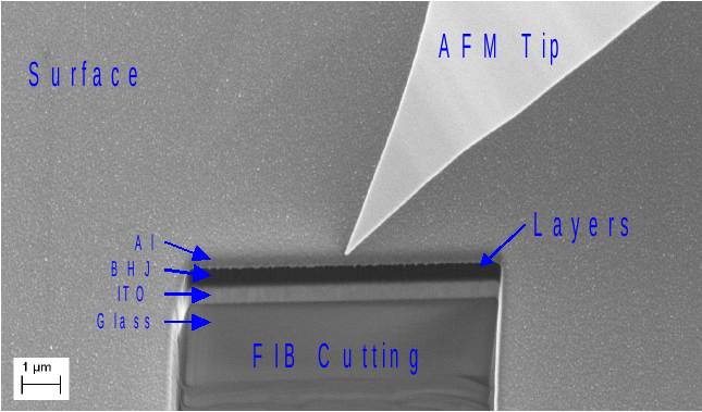
Sample after preparation by focused ion beam (FIB)
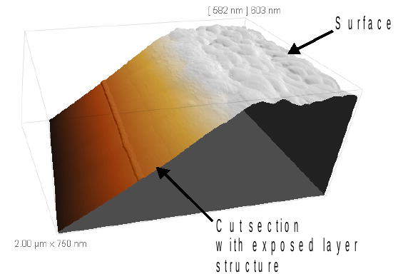 AFM micrograph showing the 3D topography of the cut out section
Reference:
1. Rebecca Saive, Michael Scherer, Christian Mueller, Dominik Daume, Janusz Schinke, Michael Kroeger, Wolfgang Kowalsky, Imaging the electric potential within organic solar cells, Advanced Functional Materials Volume 23, Issue 47, December 2013, Pages 5854-5860
Technology
SAMPLE TRANSFER SHUTTLE
|
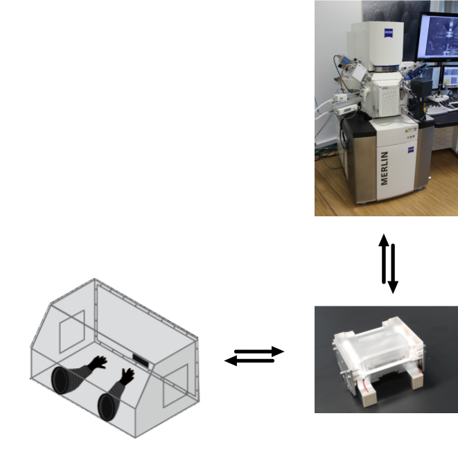
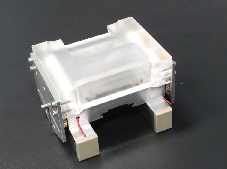
The Sample Transfer Shuttle is a small container, which allows the transfer of a sample holder from a glovebox to the SEM under controlled atmosphere or vacuum. It works fully autonomously, because it has its internal electronic an battery. No external power source or feedthroughs into the SEM chamber is required. The shuttle can be opened and closed by an infrared based remote control. The shuttle chamber can contain inert gas atmosphere or vacuum. |
 |
Intelligent Solution
| Sample transfer between glovebox and SEM is performed either in vacuum or in an inert gas atmosphere Sample Transfer Shuttle remains in the airlook. Only the sample holder is moved onto the SEM stage, thus full problem-free stage maneuverability and no shadowing by the shuttle is guaranteed Sample Transfer Shuttle is locked in and out through the airlock, thus there is no need to open the door of the SEM main chamber. |  |
FEATURES
Sample transfer shuttle is a protective solution during the research of
- battery and fuel cells,
- thin or etched films,
- organic electronics,
- some sort of semiconductors,
- hydrophilic crystals and many more, i.e. for all surfaces which should be protected from oxidation, corrosion, moisture, contamination, etc
Product Line
Sample Transfer Shuttle
|
Transfering sample easily and safely between SEM and glovebox In the glovebox or in any other inert gas environment for preparation or storage, the sample is mounted onto the sample holder. After opening the Sample Transfer Shuttle, the sample holder can be inserted into the shuttle. After this, the shuttle has to be closed. The opening and closing of the Sample Transfer Shuttle is done by remote control from outside the glovebox. Now, the Sample Transfer Shuttle can be locked out of the glovebox and mounted into the SEM airlock. After pumping the airlock to vacuum, the Sample Transfer Shuttle is opened by remote control, and the sample holder can be moved to the SEM microscope stage, using the standard ZEISS transfer rod, while the Sample Transfer Shuttle remains in the airlock. |
 |
Products

Sample Transfer Shuttle
Protect your sample from air exposure with Sample Transfer Shuttle from Semilab.
How it supports you during your research activity?
Providing reliable performance:
- Safe and easy transfer of delicate samples in vacuum or in an inert atmosphere between the SEM and the facilities for sample storage and preparation, for example a glovebox or glove bag
Ease of use:
- Infrared remote control for opening and closing the Sample Transfer Shuttle
Flexibility:
- Shuttle chamber can be filled with an inert gas atmosphere or pumped to vacuum by a manual valve
- Samples can be mounted either to standard SEM sample plugs (maximum sample size 10 mm × 10 mm × 2 mm)
or to the provided transferable holder, also used in the SEM-AFM (maximum sample size 10 mm × 10 mm × 6 mm) - Field installation possibility