


Application
CORRELATIVE MICROSCOPY
Nearly all semiconductor devices are made of hetero structures, stacked layers of different materials deposited with different techniques. Thicknesses of these layers are in the range of micrometers down to nearly single atomic thickness. For the correct operation of an electronic device, the electronic configuration at layer interfaces is essential. Even though the electronic properties of such interfaces can be simulated, many physical effects caused by the deposition process and layer interactions influence the interface in a certain and often non predictable way.
Here, we present a powerful way of performing an in situ analysis of hetero structure interfaces using an organic solar cell structure as an example. The method and the work presented here were developed and performed by Saive et al. [1]. Interfaces have been electrically characterized by Scanning Kelvin Probe Force Microscopy (SKPM). Like in a conventional kelvin probing system, the SKPM method provides information about the work function (chemical potential) difference between a sensing tip and the sample surface. For SKPM, an atomic force microscope (AFM) tip is used as a kelvin probe sensor, which allows to measure work function variations with extremely high lateral resolution, in some cases down to atomic level. The work function is determined by the intrinsic potential of a material, the electronic configuration like carrier density and type, and an eventually applied electrical potential. Performing an SKPM measurement on a cross section of a hetero structure, results in absolute measurements of work function differences between the different layers. This also enables the direct measurement of the voltage drop between the different layers if an external voltage is applied across the hetero structure.
The surface of an organic semiconductor is very sensitive to air exposure, so these semiconductors have to be encapsulated in air tight containers. To perform high resolution electrical characterization, exposed surfaces have to be protected from air contamination. The combination of the Carl Zeiss AURIGA crossbeam work station and the Carl Zeiss AFM option for MERLIN allows preparation and investigation of the solar cell without the need to expose the prepared structure to air.
The precise navigation of the AFM tip directly to the region of interest is ensured by high capability zoom of the SEM. In this way, it is possible to access information about topography, mechanical, electrical and magnetic properties of the surface with nanometer resolution.
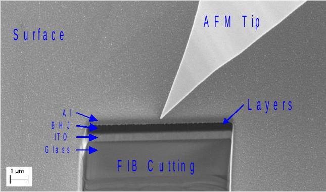
Sample after preparation by focused ion beam (FIB)
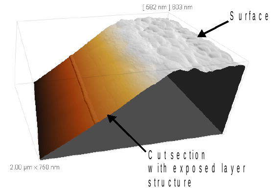 AFM micrograph showing the 3D topography of the cut out section
Reference:
1. Rebecca Saive, Michael Scherer, Christian Mueller, Dominik Daume, Janusz Schinke, Michael Kroeger, Wolfgang Kowalsky, Imaging the electric potential within organic solar cells, Advanced Functional Materials Volume 23, Issue 47, December 2013, Pages 5854-5860
Technology
SCANNING ELECTRON MICROSCOPE INTEGRATED ATOMIC FORCE MICROSCOPY (SEM AFM)
Why to combine Atomic Force Microscopy (AFM) with Scanning Electron Microscope (SEM)?
A combined SEM-AFM has a number of advantages in comparison to the two systems as stand-alone.
The system offers new possibilities for measuring surfaces and nanostructures. The combination of SEM and AFM offers an exact positioning of the AFM tip. The AFM gives you precise information about topography, electrical and mechanical properties of the surface.
APPLICATIONS:
- Surface properties analyzation like:
- Magnetic force on the sample surface
- Chemical surface potential by Kelvin Probe Force Microscopy (KPFM)
- Conductivity of the surface and many more
- Potential distribution along the layer structure of an SMD capacitor
- Topographical and electrical properties
-
Potential diffence between the two electrode materials
-
Graphene and other 2D materials
- Characterization of:
- Heterogenic structures of nanosized devices and functional structures in semiconductor
- Energy storage
- Sustainable energy production
You can read more advantages of the combined system in our article SEM and AFM – high resolution with overview.
HARDWARE INTEGRATION
Our approach to realize a combined SEM-SPM system is based on the integration of a vacuum compatible SPM into existing SEM systems. This combination was selected to reach the highest performance and usability of the system. Another benefit of this strategy is that existing SEM systems can be upgraded to a combined SEM-SPM system. In both cases, the SEM will not be limited in its function so that combined SEM/SPM measurements are possible.
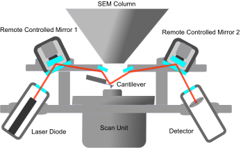
The SPM is designed as a sample scanner for integration. This design enables the alignment of the electron beam and the SPM tip with the highest precision, because the beam and the tip are not moved against each other. Even during SPM scanning, this enables unknown possibilities of combined measurements. Additionally, the highest performance can be achieved by this setup in terms of resolution and frame rate. The scan unit itself is the next developmental step of our STM scanner, known for high stability and reliability in the last decades. With a scan volume of 9 µm × 9 µm × 1 µm and a possible sample size of 10 mm, the design claim for high resolution is clearly visible. Electronic components like the laser diode, the detector and the preamplifier are located inside the vacuum chamber in hermetically encapsulated compartments. The alignment of the laser path and also the exchange of the cantilever and the sample can be performed without breaking the vacuum. The positioning of the SPM in respect to the SEM and the positioning of the SPM tip to the area of interest can be realized by a remote control. With a small number of changes to the SPM, a UHV compatible version is available.
SOFTWARE INTEGRATION
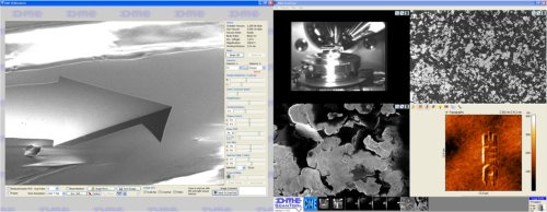
The grade of functionality of highly complex scientific instruments like the SEM-AFM, depends on the operating software. To achieve the seamless integration of the methods, a single software user interface is necessary. The open design of our SPM Software ScanTool™ enables us to integrate a self designed SEM operating software. Therefore the operator is able to control both systems from one platform and the same software without clicking through a labyrinth of tabs and windows. The view on all settings and image data of both methods is unblocked and accessible. The software is designed for the highest work flow and throughput. At the same time, program functions like the DME Automator give access to all functions of the SEM-AFM system, so user-designed advanced measurement routines can be designed and performed. Ttherefore it is possible to create automatically running measurement routines for the acquisition of comparable data from different regions of the sample. Image data from SEM and SPM are analyzed in the ScanTool™ software. Standard analyzing tools are available, more advanced or specialized analysis procedures can be implemented for ourselves, or implemented by us on customer demand by the use of the "DME Automator" or "DME Image Calculator".
For more information about the technology, product description and applications, please click here.
FEATURES
- Is based on the DME UHV AFM and the Carl Zeiss Auriga® Crossbeam Workstation.
- The crossbeam point of SEM and FIB lies at the cantilever tip. The design as a sample scanner allows combination measurements of all three techniques at exactly the same point in space and on the sample.
- Extremely stable scan unit designed for three dimensional single atomic resolution.
- Scanner Specification: Scan range (x,y,z) 10 µm × 10 µm × 1 µm, real resolution subatomic in all three dimensions.
- Single software interface for both SEM and AFM components.
- Common data storage of AFM and SEM images.
- SEM viewing angle from 0° to 85° while keeping minimum SEM working distance of 5 mm.
- Cantilever tip and sample can be reached by FIB in 0° and 54° position, in situ tip sharpening by FIB supported.
- Supports easy change between AFM and standard Auriga® functionality by user-exchangeable SEM door.
- Unlimited functionality by using all standard AFM cantilevers, no active probes required.
- Supports all common AFM operation modes.
- Automatic laser / detector alignment on cantilever change.
- Update of existing Auriga® SEMs to BRR functionality possible by simple door exchange.
Product Line
SEM-integrated Atomic Force Microscope
From millimeters to atomic level
Use the zoom capabilities of the SEM to navigate your AFM tip directly to the region of interest.
Access information about topography, mechanical, electrical and magnetic properties of the surface with nanometer resolution.
Use the AFM tip as a nanomanipulator with force feedback.
The AFM is available for Merlin and Crossbeam series (other Zeiss SEM series on inquiry). Already existing systems can be updated by simply exchanging the door.
Products

SEM-AFM
In-situ AFM solution is combined with scanning electron microscope (SEM) or focused ion beam-SEM (FIB-SEM) in a single equipment.
Reliable performance provided by:
- SEM guided positioning of AFM tip to area of interest
- Anchored stage technology for ultra high stability and low drift
- In-chamber integration for simultaneous AFM and SEM imaging
- The system is controlled by the C26-Controller of Semilab and the Scan-Software ScanTool™
Ease of use:
- One software interface to operate AFM and SEM
- Automated laser and detector alignment
Flexibility in components:
- Sample scanner setup with 9 µm or 25 µm scan range
- Sample size up to 10 mm
Versatility:
- All commercial cantilevers compatible
- Capable of performing all the commercially available scanning probe microscopy (SPM) modes:
DC mode, AC mode, Magnetic Force Microscopy (MFM), Kelvin Probe Force Microscopy (KPFM), Scanning Capacitance Microscopy (SCM), Electrostatic Force Microscopy (EFM), Scanning Tunneling Microscopy (STM), Scanning Spreading Resistance Microscopy (SSRM), Lithography - Sample Transfer Shuttle