Application
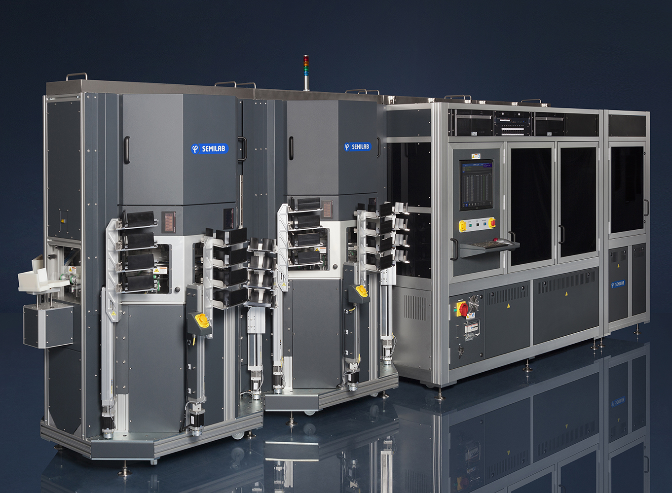
SI WAFER SORTING
Sorter applications provide advanced multiparameter wafer inspection with integrated high speed sorting for quality control of production PV wafers. Owing to wide range automation module portfolio and flexible combined Semilab’s metrology modules, all customer can find perfect configuration what fulfil their production expectations.
Application area:
- Outgoing wafer inspection for wafer manufacturers
- Incoming as-cut wafer inspection for solar cell manufacturers
Sorter purpose
- Eliminating damaged wafers from further process
- Eliminating high thickness variation wafers (TTV, saw mark)
- Sorting of potentially weak wafers (microcracks) which could break in subsequent process steps
- Sorting based on resistivity, and lifetime values
- Sorting of wafers with dislocations, high contamination and vacancy density
- Wafer input: loading from cassettes or stack
- Wafer output: Sorting in different user-defined classes, collection in coin stacks
- High throughput