


Application
NANO SURFACE CHARACTERIZATION
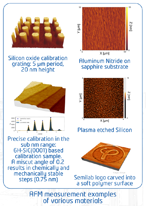
The topographical features of the surfaces in the semiconductor industry are an important source to gather information about possible failure sources or estimate success rates to improve the overall yield of the process. Therefore the investigation of the smallest surface features of silicon substrates, as well as patterned wafers can be found in a lot of applications throughout the industry.
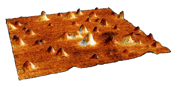 Figure 1. Surface features
Technology
SCANNING PROBE MICROSCOPY (SPM) FOR R&D
The maximum obtainable magnification with a conventional optical microscope is approximately 800-1000× due to the nature of light. For further magnification there are Scanning Electron Microscopes (SEMs) used, and among these, the Transmission Electron Microscopes (TEMs) can show single atoms and thus provide the highest possible magnification. Why do we have then the Scanning Probe Microscope (SPM) as yet another type of microscope?
One of the reasons is that a sample to be examined in a transmission electron microscope must be sliced thinly and thus ruined. The SPM technique images surface structures with atomic (height) resolution without the necessity of damaging the sample. A further reason is the kind of imaging offered by SPM microscopes, because the results are shown as a kind of three dimensional image (also in cases where only two dimensional information is evaluated). As this is the case with an optical microscope, it is very difficult to investigate the surface structure of a sample with an electron microscope. In order to measure a surface profile with the highest resolution, it is necessary to slice the sample. Moreover, an SPM operates without vacuum, and unlike electron and optical microscopes, it can measure other physical effects. This includes electrical properties, such as Kelvin Probe Force Microscopy (KPM / KPFM) or magnetic properties (Magnetic Force Microscopy, MFM).
TYPES OF SCANNING PROBE MICROSCOPES
DC MODE
The most basic AFM operation mode is the so-called DC, or contact mode. A force is applied to the cantilever (sensing) tip when the cantilever and the sample surface are close to each other. This leads to the bending of the cantilever, which changes the reflectance angle of the detection laser. The deflection of the laser is measured by a position-sensitive photo detector. When the cantilever is moved towards the sample during the approach, attractive forces are applied to the cantilever. These negative forces can be used to perform a surface scan.
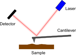
DC MODE
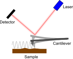
AC MODE
AC MODE
In order to prevent the cantilever from damages, most AFM microscopes are now usually operated in the so-called AC mode instead of DC mode. In this mode, a very low force is used during the scanning, and a very little interaction occurs between the surface and the cantilever without resolution loss.
The cantilever is permanently vibrated with its resonance frequency. This oscillation leads to a periodic bending of the cantilever, which is measured by a reflected laser beam like in DC mode. When the cantilever is close to the surface and interacts with the surface atoms, the resonance frequency changes. (Actually the resonance frequency increases when the cantilever reaches the surface.) This leads to the dampening of the amplitude and a phase change of the cantilever oscillation. The tip-sample interaction force and the dampening of the cantilever oscillation are approximately proportional when the tip is close to the sample.
AC mode works with less interaction force than the DC mode and has some advantages:
- The surface itself is much less influenced by the measurement because of the low interaction forces.
- Because of the lower forces, a single cantilever can normally be used for more images.
- Fragile samples, which would be destroyed in a DC measurement can be imaged in AC mode.
- The relation phase shift / damping is characteristic for the surface material, therefore more information can be gained from this operation mode.
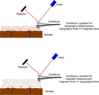
MAGNETIC FORCE MICROSCOPY - MFM
To be able to detect magnetic forces, a cantilever is to be used, which is applied with a magnetic coating. Standard MFM tips have a magnetic coating with a relatively large thickness of around 40 nm. The high thickness results in a much larger tip radius of around 50 nm. This is much larger than that of conventional AFM tips. With these standard tips, the lateral magnetic resolutions of about 100 nm can be obtained. Therefore the magnetic resolution is much less than the commonly expected resolution from AFM topography measurements, which are a factor of 10 better.
When the MFM tip is close to the sample, mechanical force, as well as magnetic force contribute to the force that is measured by the cantilever. The magnetic force is much smaller than the mechanical force, but is effective over a long distance. To separate the two force sources, the MFM force must be measured from a certain distance of the sample surface, where the contribution from the mechanical force can be neglected.
MFM
KPFM
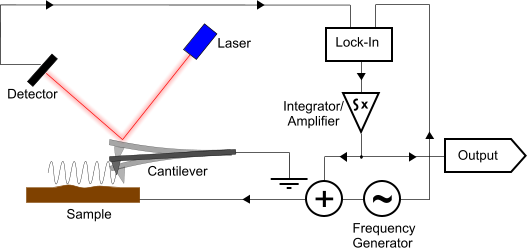
KELVIN PROBE FORCE MICROSCOPY - KPFM
This mode is a method to determine the chemical potential between a cantilever and a sample surface, and therefore receive information about the material and the material state on a sample surface. The basic setup for a KPFM measurement is shown on the figure beside. The sample is electrically connected to the output of a frequency generator. This creates an oscillating electrical field between the cantilever and the sample, which can be measured by the position sensor of the AFM. This detected signal is then fed into a lock-in amplifier and its output is put into an integrator. The result is then added as a constant offset to the oscillation, which is applied to the sample. This acts as a feedback loop, which minimizes the electrically induced cantilever oscillation.
SCANNING CAPACITANCE MICROSCOPY - SCM
This method is used to determine the relative changes of majority carrier concentration of flat semiconductor surfaces. The capacity measurement is done quite similar to the KPFM measurement. You can use the same measurement setup. The main differences are that the output is coming from the lock-in amplifier, not from the feedback signal, so one uses the force component F2ω, described above at KPFM, which is proportional to the capacity C between tip and sample surface.
The capacity measurement also results in relative information about the capacity. The absolute capacity between tip and a conducting sample is in the range of aF (atto farad = 10^-18 farad) where the capacity between cantilever body and sample is in the range of fF (femto farad = 10^-15 farad). These small dimensions and the large offset show that a direct measurement of the capacity is nearly impossible and also there, only relative values can be obtained.
ELECTROSTATIC FORCE MICROSCOPY - EFM
A KPFM measurement of the electrostatic force without a nulling feedback regulator is called EFM, electrostatic force measurement. Here, the feedback regulator is left out and the output of a lock-in amplifier is directly monitored. This measurement shows, as seen in the equation Fω derived above for KPFM, a mixture of different information and is influenced by the chemical potential, the oscillation voltages, the capacity etc. Therefore the EFM method is less useful for determining physical properties than the KFPM method.
SCANNING TUNNELING MICROSCOPY - STM
The STM mode has the most simple principle and works only with conducting samples. A metall tip perpendicular to the sample surface is used instead of a cantilever. The tip as well as the sample are connected to a voltage supply. Now the STM tip is brought so close to the sample that a current flows, a so-called tunnel current. There is an exponential connection between the tip to sample distance and the current flow.
There are two variations for scanning: In the constant height mode, the height of the tip and the voltage is kept constant, while the tunneling current changes. For an images, this changes are translated to topography information. In the constant current or feedback mode, the tip is moved up and down to maintain a constant tunnel current, thereby the tip is moving in a constant distance to the surface. The necessary up and down movements of the tip are electronically recorded and can be displayed as an topography image.
Even though this principle is very simple, it instantly delivers the maximum possible magnification and allows the investigation and manipulation of individual atoms. The reason for this is a kind of self-focusing effect: The tunnel current responsible for the imaging already flows over the atom on the tip which is closest to the sample surface. So even when using a tip cut just by an ordinary pair of pincers one quite often gets atomic resolution.
The voltages used for STM measurements are normally below 1 V, since the electric field between sample and tip created by the fine tip is very large. An applied voltage of 5 V already results in a strong electric field causing a displacement of the tip and the sample surface. Actually, a 5 V pulse is often used for "cleaning" the tip.
The tunnel currents are on the nA scale, and the distance between tip and sample are in the order of magnitude of a few nm. STM measurements require that the sample surface is atomically "clean". In air, it is only possible to obtain atomic resolution for certain samples. The easiest atomic grid to observe is that of an HOPG sample (Highly Oriented Pyrolytic Graphite) since the top layer from such a sample can be removed by means of a piece of adhesive tape, revealing for a short time an atomically "clean" surface. Therefore, such samples are often used as test structures for STM microscopes; all DME STMs are tested for atomic resolution with a HOPG sample as a part of our internal certificate of complience (CoC) test.
The STM scanning is very fast; for atomic resolution images you can usually achieve a scan rate of multiple images per second.
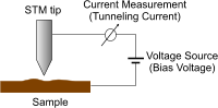 Figure 7. STM MODE
SCANNING SPREADING RESISTANCE MICROSCOPY - SSRM
In this method also an conductive probe is used. Operating in DC mode, an DC bias is applied and the electric current between the tip and the sample is measured. The resulting resistance is caused by the spreading resistance and resistivity of the sample which also give information about the carrier distribution.
Note, that you have to scratch the surface of the sample with the tip to get a better electrical contact.
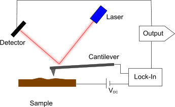 Figure 8. SSRM MODE
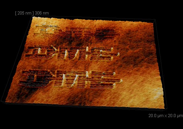 Figrue 9. Lithopgraphy example (1)
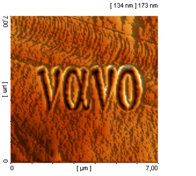 Figure 10. Lithopgraphy example (2)
LITHOGRAPHY
The typical radius of SPM sensors is in the order of 10 nm. So it is possible to perform lithography on a scale of only a few nanometers.
Doing a lithography means that physical or chemical properties of a sample's surface are being changed. This can be done in three different ways:
- exposing the sample with light or electrons,
- applying high pressures (scratching),
- applying electrical fields.
The main idea of the SPM program lithography function is to transfer the information of a bitmap via physical properties like a force, a voltage or a current to the surface. Depending in which mode (AFM-AC, AFM-DC, STM) the SPM is running, the physical property can be a bias or a current (STM), a force variation (AFM) or voltage at the auxiliary port of the controller (all modes). The Aux voltage can be converted into many other physical properties using external equipment.
Assume the surface of an AFM tip to about 100 nm2. If a tip with a force constant of 50 N/m is pressed 200 nm towards the surface, the resulting force equals about 10-5 N. The pressure applied to the surface is of about 100 GPa. This means that on almost any surface softer than the silicon tip, patterns may be scratched into the surface.
For more information read about the Scanning Probe Microscopy technology and about application examples.
FEATURES
Almost all Scanning Probe Microscopes are capable of resolving atomic height steps.
- Atomic Force Microscopy (AFM) can reach a lateral atomic resolution.
- AFM with lateral atomic resolution is only used for special cases, where achieving a lateral atomic resolution is more important than the loss of flexibility, brought on by the higher stability of the total set-up.
- Normal AFMs are designed for relatively large scan areas and the scanner stages allow investigation of many different sample types and sizes.
- Scanning Tunneling Microscopy (STM) has the advantage that the tunnel current always flows directly over the next atom on the sample surface. This kind of "self-focusing" does not occur with an AFM.
- STM is often used in ultra-high vacuum so that a prepared sample surface may remain uninfluenced for a longer time.
- STM is usually integrated into a highly stable scan platform.
Product Line
Semilab AFM Proberstation Series
With the Semilab AFM Proberstation series, we provide the ultimate unification of ease of use and performance. Decade-lasting experience in the Scanning Probe Microscopy application field and manufacturing are united in the Semilab AFM scanners to help the user achieve the best and most reliable results in the shortest possible period of time. The compact design of the Semilab AFM scanner guarantees outstanding stability and scan rates. The unique plug and play cantilever exchange secures the fast and safe operation of the instrument. An integrated optical axis in the AFM scanner provides total visual control during approach and positioning. The Semilab AFM scanner provides the facilities for all common and advanced AFM modes. The integrated electronics in the scan head guarantee the lowest noise values in electrical AFM modes. Semilab AFM Proberstation series allows the installation of the Semilab AFM scanner into the stages and other facilities, like nanoindenters or optical microscopes.
Products

AFM-2000
Atomic Force Microscope - AFM-2000 is an automated high-end Scanning Probe Microscopy platform for large samples.
Its long range XY translators allow the investigation of up to 200 mm samples and fragments at all positions. The fully programmable sample positioning enables autonomous AFM measurements on multiple sample positions with automatic image analysis and automatic report generation. The combination with high end optics enable on automated preselection of sample sites for SPM investigation.
Thereby the Semilab AFM-2000 setup is the optimal solution for industry quality maintenance application and R&D environments.
High performance:
- Lowest noise
- High precision stage, high precision motors and optical reference feedback system
- Acoustic enclosure
- Camera system for visualization of the scan area.
Ease of use:
- Cantilever exchange
- Full automation capability with in-built active vibration isolation
Flexibility:
- Automated tip exchange
- Sample size up to 200 mm
Versatility:
- Offers flexibility with AFM tip scanner setup for a wide scanning range.
- Customer-specified modifications
- Combination with other analytical heads

AFM-1000
State-of-the-art tabletop AFM with automated measurement features
High-resolution, sub-atomic precise measurements with extremely low noise level, enabling sub-atomic precision measurements and highly reproductible material characterization of various samples with up to 65x65 mm in size.
With cutting-edge technology and decades of knowhow, the Semilab tabletop AFM system enables consistent nanotopography measurements and electrical characterization of various materials, and with that, provides to your academic research microscopic measurement solutions based on semiconductor industry standards.
High Performance:
- Sub-atomic resolution AFM system
- AFM scanner utilizing flexure-guided piezo positioners for flat scanner movement
- Configurable scan area size
- Integrated dual focus camera system for laser alignment and tip-to-sample positioning
- Manually adjustable laser path
- Motorized sample stage
- Sample holder: clamps or magnetic fixing
Benefits:
- Compact tabletop AFM system with small footprint for R&D applications
- Easy and safe sample and cantilever handling
- High level of automation: series of different measurements can be automatically carried out on a single sample
Scan Area Customization Options:
|
|
Option 1 |
Option 2 |
|
Scan range |
50x50 µm |
100x100 µm |
|
Z range |
5 µm |
10 µm |
|
Stage range |
20x20 mm |
|
Request Info

AFM-2100 Atomic Force Microscope
Semilab Atomic Force Microscopes provide high-resolution, sub-atomic precise measurements with extremely low noise level which enables consistent and highly reproducible roughness characterization for the quality control of Si and compound wafers. AFM-2100 offers state-of-the-art metrology solutions for those seeking atomic force microscopy with manual sample loading, providing flexibility and hands-on control.
The Semilab AFM-2100 system is designed for various applications, including:
- CMP Process Control:
- Analysis of micro-roughness and lateral surface structures
- Automated Defect Review:
- Defect detection by light-scattering method (μPIT) and characterization using AFM
- Device Characterization:
- Critical Dimension measurements, failure analysis
Key Features:
- AFM Tip Scanner, utilizing flexure-guided piezo positioners for flat scanner movement
- Fully automated AFM with manual sample loading
- Automatic tip exchange and laser alignment
- Sub-atomic resolution
- Maximum scan area size can be configured according to industry requirements
- Full 12-inch wafer is accessible by the AFM scanner
- KLARF file import & export
- Profilometer mode
- Optional Advanced Defect Review, Heated stage and Visualization Camera