


Application
INLINE PROCESS CONTROL
Besides Semilab’s own automated wafer sorter platform, Semilab manufactures separate measurement units for integration into automated PV production lines. Semilab has been working together with all the relevant automation companies to integrate the measurement units.
The equipments cover a diverse range of metrology needs for comprehensive process and quality control in Si PV industry:
- Incoming wafer inspection and process control during cell manufacturing
- Measurement in as-cut wafer, textured, after diffusion, after passivation, after ARC deposition, after contact formation states
- Measurements of geometrical, electrical and optical properties
- Solutions for mono and multicrystalline silicon materials, Al-BSF, PERC, IBC and heterojunction cell concepts
All measurement units are designed considering the following directives:
- Compatibility to state-of-the-art production lines
- Supporting all the industry standard communication protocols
- Flexible integration
- Supporting both „on-the-fly” and „stop-and-go” data acquisition modes
- Compact design
- Simple integration and support
- Simple maintenance, rare calibration periods
- Application of noise reduction solutions
- Simple and configurable customization of communication protocols
Technology
SHEET RESISTANCE MEASUREMENT
The combination of the ion implant process and the process to anneal implants is usually monitored by measuring the sheet resistance of the implanted layer. The sheet resistance varies with dose, energy, and the amount of implanted species that has become electrically active. It is the sheet resistance that ultimately determines the device performance. Thus, measuring sheet resistance is an excellent way to monitor everything associated with an implant process.
The basic idea of the JPV method is the light excitation of the np or pn layer structure, and the pick-up of the resulting junction photovoltage by a capacitive probe. The detected potential is determined by the sheet resistance of the implanted layer, capacitance of junction and resistance through over the diode.
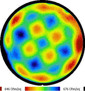
Figure 2. Sheet resistance measurement (lower range)
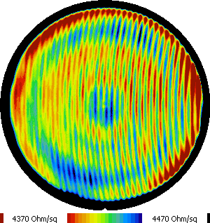
Figure 3. Sheet resistance measurement (higher range)
Semilab offers JPV technology to make non-contact, high resolution fast maps of sheet resistance.
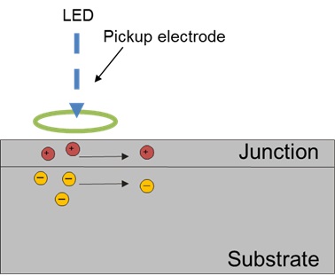
Figure 4. Measurement theory
MEASUREMENT THEORY:
The sample is illuminated by chopped LED light, which generates electrons and holes in the substrate layer. The generated charge carriers diffuse to the junction and the electric field located in the junction separates them. The result of the separation is the change in the junction voltage. This voltage change spread laterally in the implanted layer and the attenuation depends on the sheet resistance, junction capacitance, resistance of the junction and chopping frequency of the LED.
The potential change is detected by a capacitive sensor in order to evaluate the JPV signal, as a function of the frequency of the emitted light.
Based on the evaluation, the sheet resistance (Rs), capacitance of junction (Cd) and the resistance of the diode (Rd) can be calculated.
The junction leakage current is directly connected to the Rd by the following equation:
I_L=kt/q/R_d
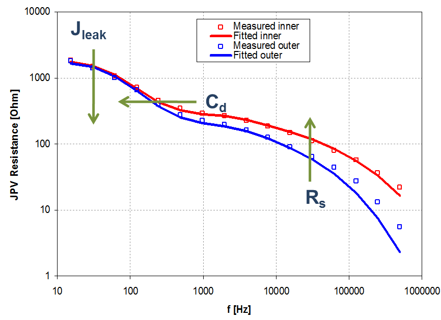
Figure 5. The detected potential is determined by Rs, Cd, Rd and frequency
FEATURES
- Non-contact, non-destructive
- No probe conditioning
- No sample preparation needed
- Works through oxide or coating
- High resolution mapping capability
- Fast mapping
- Good repeatability
Product Line
CMS, CLS
Light sources: monochromatic LED, wavelength depending on junction depth
Resolution in X-Y mapping: single point measurements at predefined points
Samples: np or pn structure (diffused or implanted USJ)
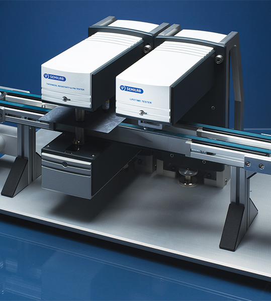
Products

CMS, CLS
FAST NON-CONTACT MATERIAL CHARACTERIZATION AND PROCESS CONTROL
Emitter sheet resistance is a primary quality control parameter for silicon wafers in PV applications after emitter diffusion.
The CLS models, CLS-1A, CLS-3A, and CLS-5A, Emitter Sheet Resistance Testers allow measurement of sheet resistance at 1 to 5 points with the high throughput that meets the requirements of in-line quality control in fully automated cell production lines.
The CMS models, CMS-1A, CMS-3A, Emitter Sheet Resistance Testers allow measurement of wafers “on the fly”, i.e. conveyor belt does not stop during measurement. Therefore, they have the high throughput that meets the requirement of in-line quality control in fully automated cell production lines.
Featrues and System specifications:
- Meas. technique: non-contact, junction photovoltage (JPV)
- Sample size: 100 to 156 mm (210mm option)
- Sample structure: np or pn junctions
- Probe distance: 1.5 mm probe height above transport bel
- Sample support: on belt
- Calibration: by wafers verified with four point probe
Options:
- Measurement module (incl. 1A-5A sheet resistance measurement heads)
- Industrial PC (Windows operation system) and peripherals
- CLS-1M emitter checker – option
- Wafer presence sensor (CMS only)
Wide variety of available interfaces to automation and MES:
- 24V optically isolated I/O, Ethernet interface
- Profibus
- OPC DA
- TCP/IP protocol, content can be XML or ASCII
- SQL database
- SECS/GEM