


Application
INLINE PROCESS CONTROL
Besides Semilab’s own automated wafer sorter platform, Semilab manufactures separate measurement units for integration into automated PV production lines. Semilab has been working together with all the relevant automation companies to integrate the measurement units.
The equipments cover a diverse range of metrology needs for comprehensive process and quality control in Si PV industry:
- Incoming wafer inspection and process control during cell manufacturing
- Measurement in as-cut wafer, textured, after diffusion, after passivation, after ARC deposition, after contact formation states
- Measurements of geometrical, electrical and optical properties
- Solutions for mono and multicrystalline silicon materials, Al-BSF, PERC, IBC and heterojunction cell concepts
All measurement units are designed considering the following directives:
- Compatibility to state-of-the-art production lines
- Supporting all the industry standard communication protocols
- Flexible integration
- Supporting both „on-the-fly” and „stop-and-go” data acquisition modes
- Compact design
- Simple integration and support
- Simple maintenance, rare calibration periods
- Application of noise reduction solutions
- Simple and configurable customization of communication protocols
Technology
CARRIER LIFETIME (µ-PCD, QSS-µPCD)
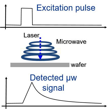
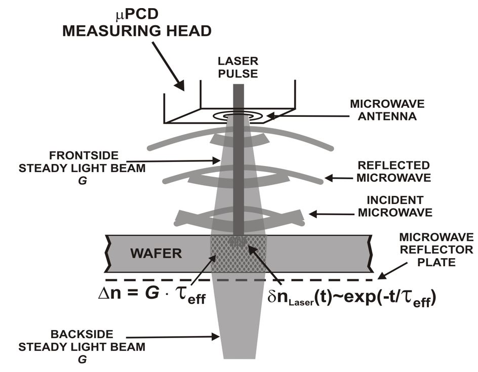
Microwave detected PhotoConductance Decay (µ-PCD) Carrier lifetime measurement is a useful technology for incoming wafer inspection, quality control and process monitoring in wafer manufacturing as well as in solar cell manufacturing. The microwave induced photoconductive decay method is the most common way of measuring minority carrier lifetime in silicon. This method excels due to its reliability, good reproducibility and the short measurement time that permits of making lifetime maps with high resolution.
Frequent contaminants and their lifetime killing efficiency:
|
Level of influence |
Element |
|---|---|
|
Strong |
Fe, Pt, Cu |
|
Medium |
Pd |
|
Weak |
Mo, W |
|
Negligible |
Ca, Al, Zn, Ti |
A contaminant may exist in two molecular states, with different effects on lifetime (or diffusion length).
The change in lifetime, caused by changing the state of the contaminant, measures the amount of that contaminant:
- Requires a unique method of changing states
- Constants are derived empirically
- The effect of a contaminant on lifetime may be dependent on injection level
- Change can be detected by μ-PCD or SPV technique
µ-PCD technique
It is a metrology of recombination properties and defects used in silicon photovoltaics and IC manufacturing as well. The technology is based on pulse of laser light, which generates carriers. Excited carriers change the conductivity of semiconductor. The microwave reflection is sensitive to change in conductivity measured signal shows decaying of conductivity. The objective of the monitoring is the bulk lifetime parameter, because that gives information about the contaminations and dislocations.
Role of Crystallinity in case of Multicrystalline Silicon:
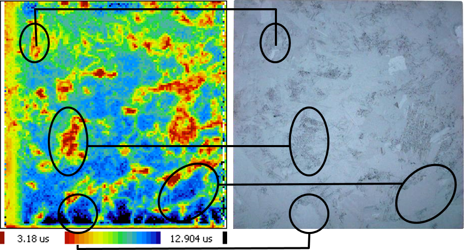
Different lifetime can be observed on different grains
Quasi-Steady-State Microwave detected PhotoConductance Decay
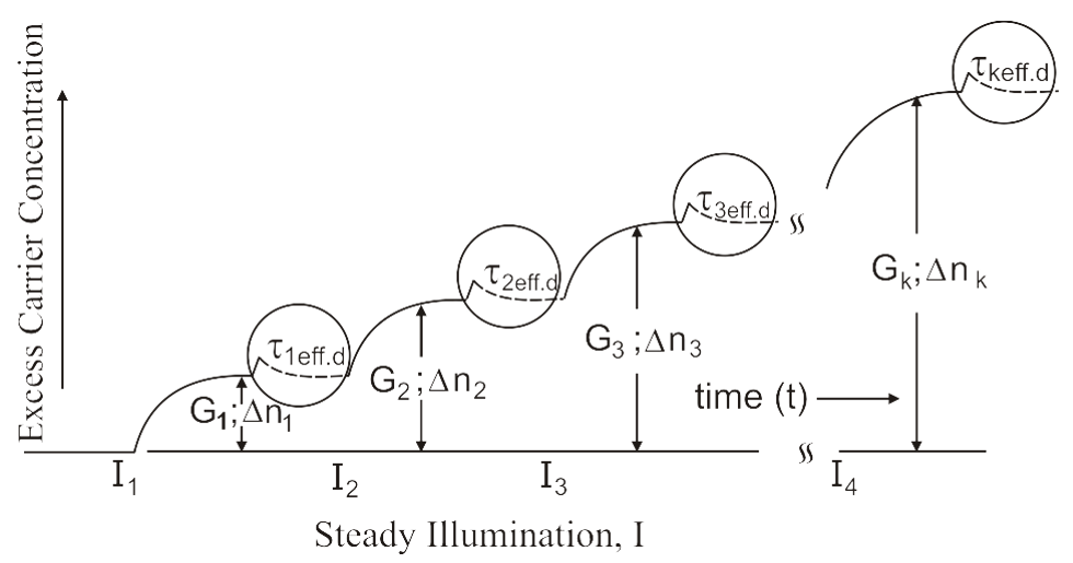
A new powerful version of the technique introduced by Semilab is termed, QSS-μPCD with QDC i.e. the Quasi-Steady-State Microwave (detected) Photoconductance Decay with Quality of Decay Control. It gives enhanced accuracy, new capabilities and broader applications. The technique represents a unified lifetime measurement for silicon PV wafers that enables self-consistent parameter-free determination of two lifetimes most-frequently used in solar cell manufacturing, i.e. the excess carrier decay lifetime, Ʈeff.d, and the quasi-steady-state effective lifetime, Ʈeff.ss. This provides a basis for determination of other recombination parameters important for PV over a broad range of steady-illumination. The technique retains unique wafer mapping advantages of μ-PCD.
In QSS-μPCD technique a decay lifetime measurement is done using a small perturbation transient condition imposed on the steady-state condition. The steady light is turned on to achieve the steady-state condition. Then the short laser pulse generates additional free carriers, and their decay is monitored to determine the decay time constant.
The laser excitation is small compared to steady-state carrier excitation small perturbation condition is well satisfied.
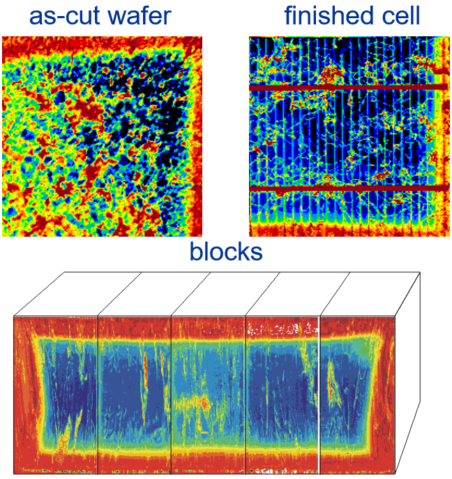
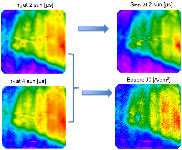
Example of typical QSS-µPCD maps:
FEATURES
- Suitable material to measure:
- Blocks
- As-cut wafers
- Lapped wafers
- Diffused wafers
- Coated wafers
- Finished cells
- Mono-, multicrystalline and EFG material
- Parameter free, non-contact method, suitable for mapping
- Small laser spot diameter
- Suitable material to measure: Passivated surface Si wafers with QSS-µPCD
Product Line
WML, WLL
Measurement technique is µ-PCD, which is applicable for incoming wafer inspection, sorting and after emitter diffusion for efficiency prediction.
Products

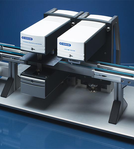
WT-2010D
The WT-2000D is a complete measurement tool for monitoring quality of silicon blocks by measuring Carrier recombination lifetime and resistivity. The system provides fast, non-contact measurements (single-point, line scans and/or maps) on silicon blocks in size up to 210x210x500 mm. It has manual and automatic measurement modes and manual block loading capabilities.
Carrier recombination lifetime is a primary quality control parameter for multi-crystalline silicon blocks. The measurement is based on µ-PCD technique.
Resistivity is measured based on eddy current technique.
Request Info
WT-2000PVN
The WT-2000PVN is a table top measurement system, capable of performing a variety of measurements on PV cells, wafers, and blocks. The base system includes the overhead functions, and you configure the measurement capabilities to match your specific needs, by selecting from the options below.
The WT-2000PVN can measure blocks and ingots, as well as wafers and cells. For measuring wafers and cells, people typically produce maps. When measuring blocks or ingots, people often produce only line scans, to save time, WT-2000PVN can do both.
Most producers of PV cells own a WT-2000PVN. It is extremely useful for:
- Engineering development and characterization
- Batch testing of production
- Comprehensive troubleshooting of production problems
Measurement techniques that can be integrated in WT-2000PVN:
- µ-PCD / carrier lifetime
- Measured parameter: carrier lifetime
- High resolution mapping and discrete point measurements
- SHR / sheet resistance
- Measured parameter: emitter sheet resistance
- Mapping and discrete point measurements
- LBIC / photovoltaic response, quantum efficiency, diffusion length
- High resolution mapping with 1 to 4 lasers
- Measured parameters:
Short circuit current
Direct and scattered reflectance
IQE and EQE
Diffusion length
- Eddy current resistivity
- Non-contact resistivity mapping
- Different resistivity range probes
- Bias light to µ-PCD