


New product release: SRP-2100i Spreading Resistance Profiling system with I-V capability
05.27.2021
We are pleased to present Semilab’s new metrology system: Spreading Resistance Profiling with I-V capability (SRP-2100i).
 SRP-2100i, Semilab’s latest Spreading Resistance Profiling (SRP) system combines standard SRP technique with optional Point-Contact IV (PCIV) method. Therefore, SRP-2100i is capable of characterizing layer structures and monitoring profiles of different compound semiconductors in a wide resistivity range, while keeping the well-established dual-probe method for determining resistivity and carrier density profiles in all silicon structures.
The system is ideally suited for easy failure analysis of fabrication processes and doping operations including epitaxial growth, ion implantation and diffusion. It is highly applicable for any silicon, compound semiconductor, SOI wafer and power device manufacturers, as well as for R&D departments.
The measurements are destructive and require preliminary sample preparation in order to determine device behavior and quality. SRP-2100i system currently has no direct competitors.
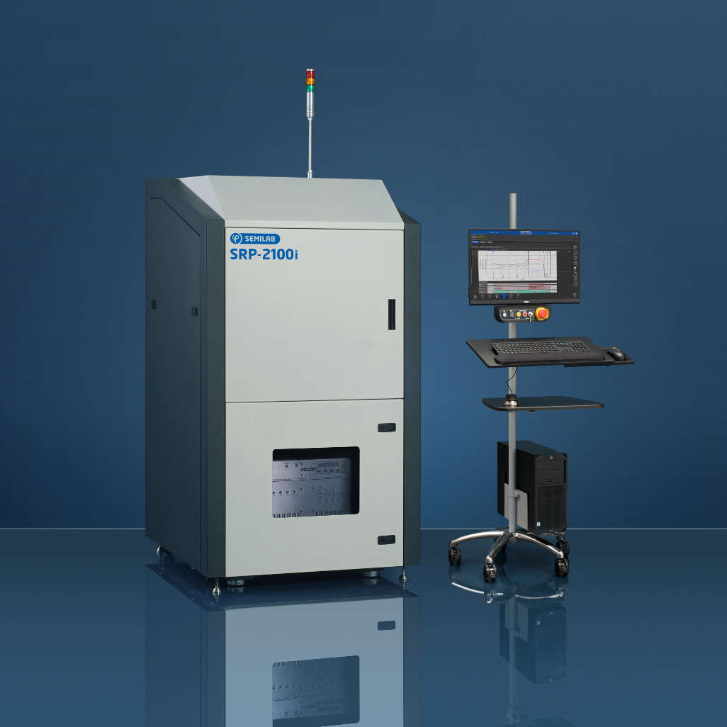
Figure 1. SRP-2100i
Applications of SRP-2100i
Various properties, electrical characterization and defects of low-energy semiconductor wafers and devices can be monitored effectively with SRP technique. It also provides useful information on resistivity and electrically active carrier density of the examined samples.
Application of PCIV technique proved to be effective at
- characterizing different device structures,
- determining layer thicknesses and
- junction locations.
Measurements showed great results on a wide variety of materials such as GaAs, Ga2O3, InP, InGaAs, AlGaN & GaN HEMT structures, also SiC power device structures (MOSFETs, SBDs). The method is capable of comparing samples with varying mole fraction ratios in case of AlxGa1-xAs and monitoring SOI or even II-IV semiconductor (ZnO, CdS) samples.
Benefits
- A versatile electrical technique for characterizing depth profiles from surface through any multilayer structures of arbitrary depth
- Offers high spatial and depth resolution
- Measurements on patterned samples are available
- Capability to measure thin layers with Shallow Layer Measurement (SLM) option
- Capability to characterize any wide bandgap, compound and SOI materials with Point Contact IV (PCIV) and iPCIV options
Download SRP-2100i Brochure
See more details about Spreading Resistance Profiling
About Semilab
We design, produce and sell metrology equipment for the characterization of semiconductor and photovoltaic materials, for monitoring the manufacturing process of semiconductor devices and solar cells, and also for R&D purposes in these areas. We offer a variety of measurement techniques; most of them are non-contact and non-destructive. Many of our technologies can be flexibly integrated into different platforms, ranging from simple handheld devices and table-top systems with high resolution mapping capability to fully automated stand-alone production control tools for mid-range and high-level fablines. We also offer in-line measurements for solar cell production lines.
Our strategy is to continuously improve our products, and to offer flexible solutions for our customers’ needs with high-value products for a reasonable price.