


Application
EPI RESISTIVITY MEASUREMENT
A blanket layer of silicon can be added to a silicon substrate by a CVD process to achieve changes in the properties, like resistivity, type and defect density. This CVD process is called epi (or epitaxial) deposition. The thickness monitoring of the epi layer is part of the production process of making the epi wafers. This monitoring is executed on a sample basis, or only to confirm that the epi reactor is set up properly.
Semilab can offer non-contact optical solution for Epi thickness monitoring, depending on infrared reflection techniques.
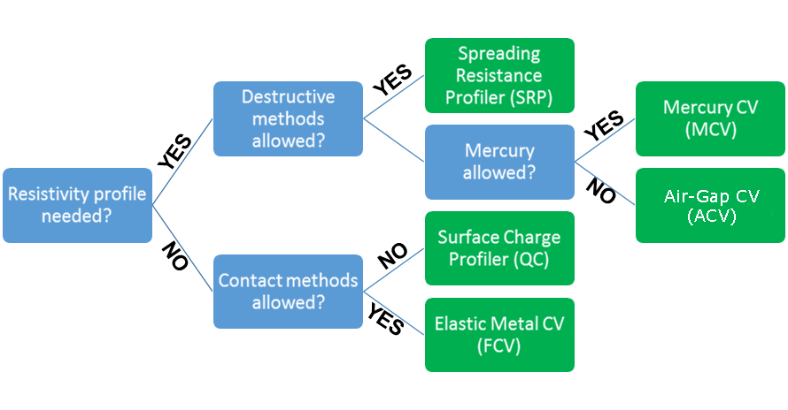 Figure 1. Resistivity measurement flow
Technology
SPREADING RESISTANCE PROFILING
Spreading Resistance Profiling (SRP) gives the user the ability to see the entire carrier density, depth and resistivity profile in a silicon device. SRP has no practical limits on carrier density range, conductivity type, orientation or profile depth. With help of SRP Designers can easily check how closely their models represent actual fabricated devices and Yield Enhancement Engineers can “fingerprint” a fabrication process for easy failure analysis. Additionally Process Engineers can troubleshoot all silicon doping operations, including: epi, ion implantation, and diffusion.
THE SRP IS BASED ON A SIMPLE, BUT VERY EFFICIENT STEPS
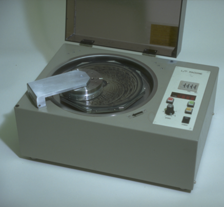
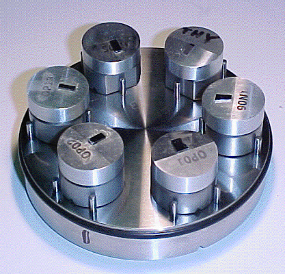
1. Probe conditioning and qualification - The contact resistance measuring method requires an ideal contact of the probe and the sample surface. In order to obtain the correct measurement outcome the surface of the probe has to be covered with microcontacts, this is the reason why the probe is conditioned with help of Gorey-Schneider Grinder.
Gorey-Schneider Grinder
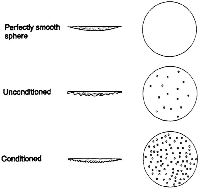
Different probe surfaces
2. Calibration (if needed) - during the measurement is obtained the Resistance value and based on the calibration curve is possible to read the corresponding Resistivity.
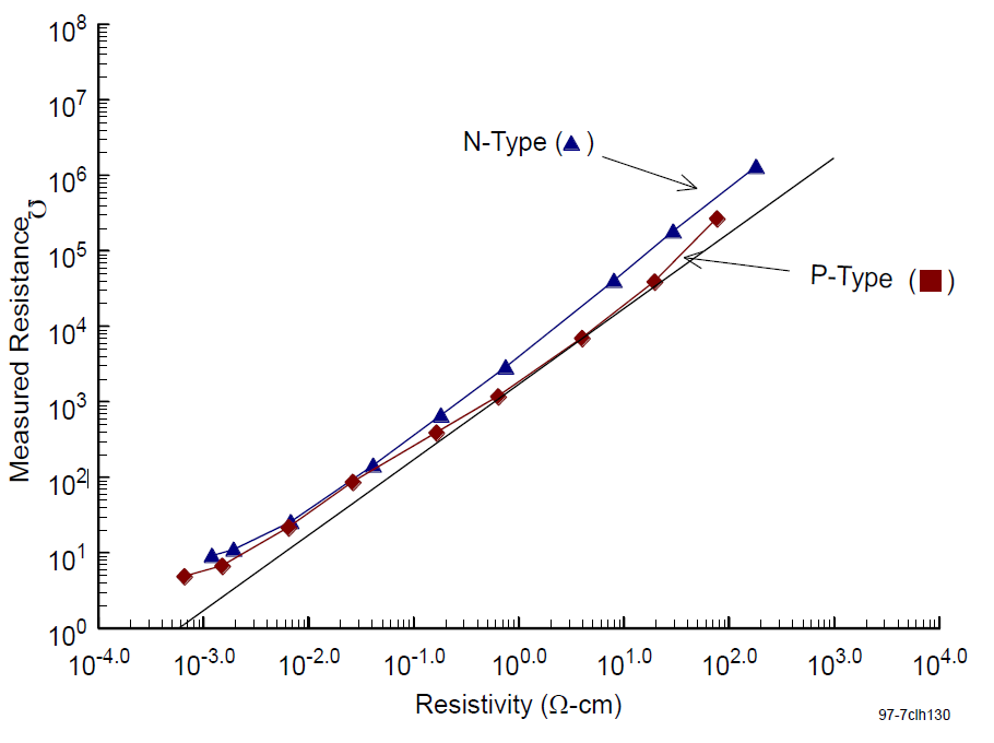
Calibration curve
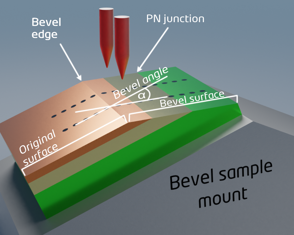
3. Sample preparation - because the resistance measurement happens on the cleaved edge of the sample, the sample has to be polished. For polishing is suggested to use a J90 polishing machine. The BSM angle depends on the inspected structure and layer thickness and the desired spatial resolution.
Polishing machine
Bevelled and mounted specimens
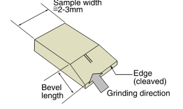
Sample with cleaved edge
4. Measurement - resistance measurement is realized alongside the bevelled edge. The built-in microscope (various magnifications available depending on tool type and configuration) gives a good opportunity to operator to easily designate the measurement path and the operator can easily avoid scratches, dirt, end of sample.
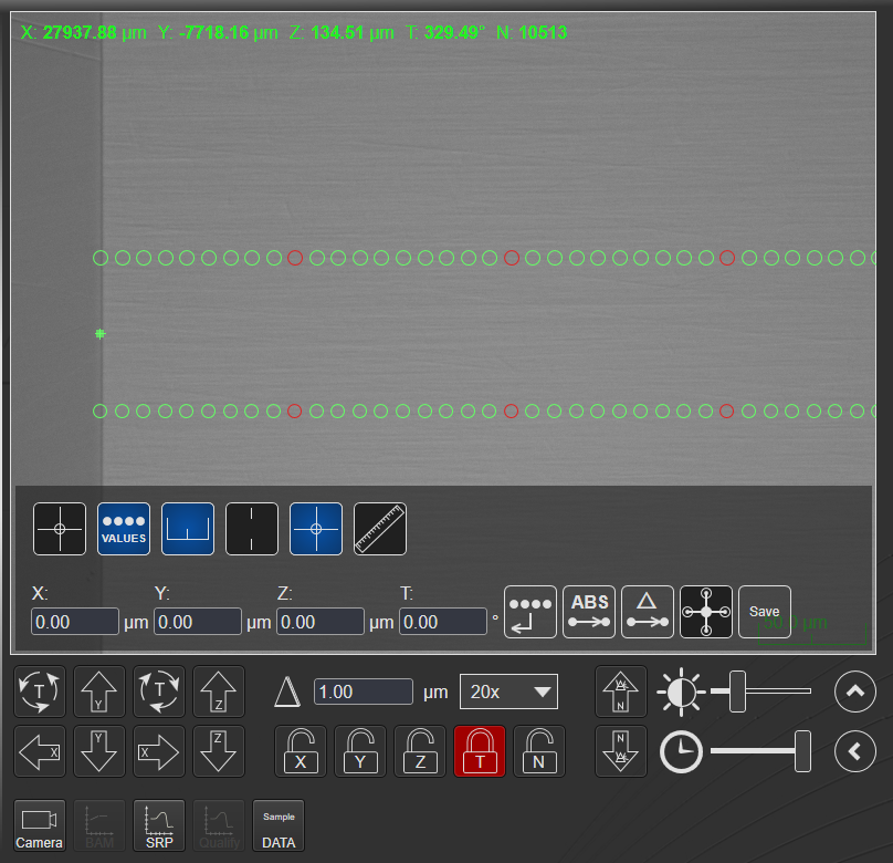
Mesaurement path(s) in the microscope
5. Analysis - The measured values can be quickly and easily analyzed with the software and is possible to realize the following:
- Locate the junctions and layers of interest
- Optional smoothing of the measured data
- Calculate the resistance and the carrier density
- Use statistics tool for layer characterisation
- Recipes available for fast evaluation and reporting
- Export data into CSV fileformat
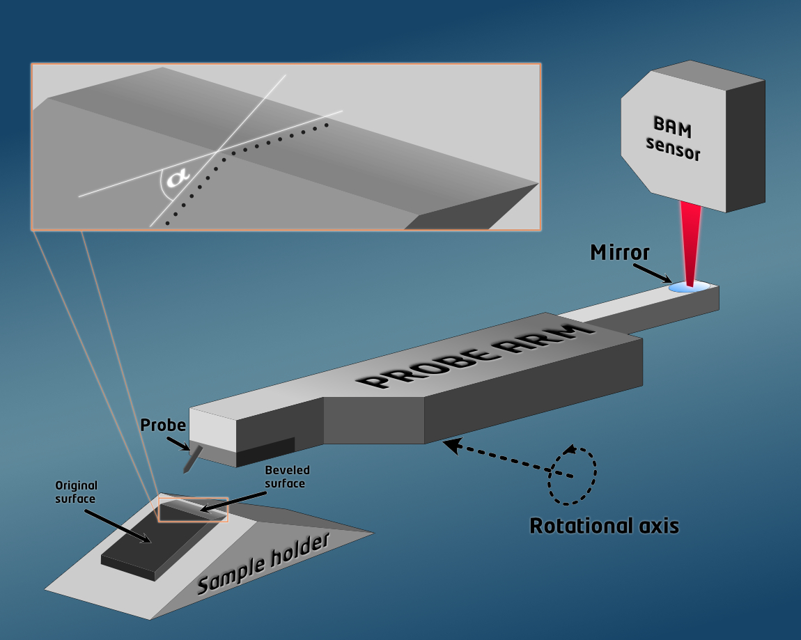
If the item of the interest is the doping level, depth of the layers, this value can be calculated from the Bevel Angle Measurement (BAM). BAM sensor senses the probe displacement on original surface compared to beveled surface. Further calculations are realized by the software.
FEATURES
- Spreading resistance profiling (SRP) enables the depth profiling of carrier density (or resistivity) across the whole layer or device
- Works on epitaxial layers, diffused layers and implanted layers
- Covers all practically used resistivity ranges
- All major epi houses and power device companies use this for
- Monitoring epi layer production
- Monitoring diffusion processes
- Failure analysis
Product Line
SRP
- A versatile electrical technique for characterizing depth profiles from surface through any multilayer structures of arbitrary depth
- Offers high spatial and depth resolution
- The technology can be used on wide range of resistivities & dopant densities
The SRP product line can be used in the following applications:
- Resistivity and doping depth profile determination in silicon semiconductor epitaxial layers
- Process monitoring of ion implantation
- Real structure determination of final devices
- Measurement on patterned samples
Products

SRP-2100 Spreading Resistance Profiler
Explore the entire carrier density and resistivity profile in all silicon semiconductor structures of device processing with this automated system. Measurement range covers state-of-the art application needs.
- Dopant concentration and resistivity
- Carrier density and resistivity profile shape
- Junction depth
- Transition width
- Sheet resistance
- Electrically activated dose
- Bevel Angle Measurement (BAM)
Features
- Ultrawide measurement range, flexible application
- High-resolution, non-overlapping measurement
- Transition zone, junction depth calculation
- In-Situ Bevel Angle Measurement (BAM)
- Low noise, ultrahigh precision stage
- Effective, high quality vibration and acoustic isolation in measurement chamber
- Touch-driven user interface and user-friendly software
Options
- P/N tester: dope and type characterisation by hot probe technique
- Shallow Layer Measurement (SLM): extending the SRP technique to determine thin layer structure
- Variable Probe Spacing (VPS): based on motorized probe spacing movement allows the measurement of sheet resistance of thin isolated layers
- Temperature Controlled Measurement Chamber (TCM)
- Signal Tower: standard industrial signal tower which gives information on system status
- Stand-Alone Bevel sample polishing unit

SRP-170 Spreading Resistance Profiler
The SRP-170 system is a cost effective, commercially available spreading resistance profiling metrology system for resistivity and carrier density profiling in all silicon semiconductor structures of device processing.
Measured parameters
- Dopant concentration and resistivity
- Carrier density and resistivity profile shape
- Junction depth
- Transition width
- Electrically activated dose
Features
- Transition zone, junction depth calculation
- Low noise, ultrahigh precision stage
- Effective, high quality vibration and acoustic isolation in measurement chamber
- Touch-driven user interface and user-friendly software
Options
- Bevel Angle Measurement (BAM): a laserbased sensor that allows the high precision measurement of the actual bevel angle of the samples for exact depth profiling
- Stand-Alone Bevel sample polishing unit

SRP-2100i Spreading Resistance Profiler with I-V capability
Explore the structure determination and profile monitoring of compound semiconductors and measurement of resistivity and carrier density profiles in all silicon semiconductor structures of device processing with this automated system. Measurement range covers state-of-the art application needs.
- Dopant concentration and resistivity on Si materials
- Carrier density and resistivity profile shape
- Resistance profile on compound semiconductors: AlGaAs, GaAs, GaN, Ga2O3, InP, SiC
- AlGaN/GaN HEMT structures
- Junction depth
- Transition width
- Sheet resistance
- Electrically activated dose
- Bevel Angle Measurement (BAM)
Features
- Ultrawide measurement range, flexible application
- High resolution, non-overlapping measurement
- Transition zone, junction depth calculation
- In-Situ Bevel Angle Measurement (BAM)
- Ready to upgrade with PCIV option
- Low noise, ultrahigh precision stage
- Effective, high quality vibration and acoustic isolation
- Touch-driven user interface and user-friendly software
Options
- PCIV option for wide bandgap and SOI application: combines variable measurement bias and current-voltage curve analysis to measure spreading resistance profile on novel semiconductor materials
- Iterative PCIV software option (iPCIV): designed to measure highly variable samples with very high resistance value (ideal below 1E-11 A current range)
- Shallow Layer Measurement (SLM): extending the SRP technique to determine thin layer structure
- Variable Probe Spacing (VPS): motorized probe spacing movement allows the measurement of sheet resistance of thin isolated layers
- Temperature Controlled Measurement Chamber (TCM)
- Signal Tower: standard industrial signal tower which gives information on system status
- Stand-Alone Bevel sample polishing unit