


Application
Technology
MODEL-BASED INFRARED REFLECTOMETRY
Model-Based Infrared Reflectometry is a thin film metrology inspection system that provides fast, repeatable, and non-destructive measurements on process wafers.
The IR series family of products uses proprietary Model-Based Infrared Reflectometry (MBIR) technology to deliver high throughput, low COO, non-contact, non-destructive measurements of the dimensions, composition and uniformity of etched structures and films used in integrated circuit manufacturing. The unique MBIR technology and analysis capability simplifies system calibration requirements and removes the effect of substrate variations for key layer measurements.
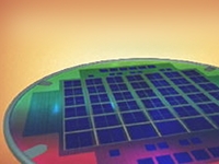 Figure 2. Patterned wafer
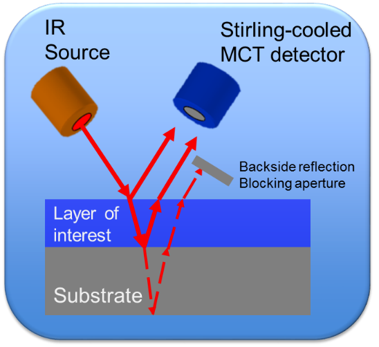 Figure 3. MBIR technology
The unique MBIR technology contains proprietary optics that suppress backside reflection and filter out extraneous data, which enhances the analysis capability, simplifies system calibration requirements and removes the effect of substrate variations for accurate and repeatable key layer measurements.
Two MBIR optics are available in two different spot size configurations:
- The large spot optics are mainly used for films or for measurements in the device area of patterned wafers.
- The small spot optics enable measurements of scribe line test structures on patterned wafers.
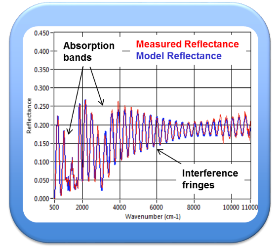 Figrue 4. Measurement results
PROCESS APPLICATIONS
The infrared spectral range is sensitive to free carriers, molecular vibrations and interference effects from the various thin films and etched structures on the wafer, enabling the technique to be employed for a wide range of semiconductor applications. By applying the effective medium calculations for 3D structures the technique has capability to scale with future technology nodes.
| Memory Applications |
|
|
|---|---|---|
| Doped EPI and Implant Applications |
|
|
| HAR Trench and Via Applications |
|
|
| 3D Integration Applications |
|
|
| BEOL Film Applications |
|
|
| EPI Applications |
|
FEATURES
- Non-contact, non-destructive optical measurement method
- Model-based technique
- High throughput
- Mid-IR to Near-IR wavelength range enables key applications
- Proprietary optics that eliminate backside reflection for high accuracy
Product Line
IR
The Semilab AMS IR family of products uses proprietary model-based infrared reflectometry to measure thickness, depth and parameters of etched and recess filled trench structures with nanometer precision. It can also measure epitaxial layer thickness with angstrom precision even at 30 nm and below.
Products

SEIR-3000
The SEIR-3000 uses proprietary model-based infrared reflectometry (MBIR) and Spectroscopic Ellipsome-try (SE) technology to deliver high throughput, low COO, non-contact, non-destructive measurements of the 3D geometry structures and uniformity of doped epitaxial layers and films used in integrated circuit manufacturing. The small spotsize makes the tool suitable for measurements of scribeline test structures. The unique hybrid SE-IR technology and analysis capability of the SEIR-3000 enables measurement capability of challenging structures and film stacks.
Features and System specifications:
- Scalable measurement capability at all technology nodes
- Capable of mixed 150/200 mm or 200/300 mm operation under software control
- Windows-based software with menu-driven recipe selection/generation
- Cognex Patmax© pattern recognition
- Camera-based autofocus

IR-2100, IR-2200, IR-2500, IR-3200
Extended wavelength model-based infrared reflectometry with high throughput, low COO, non-contact, non-destructive measurements of thickness and uniformity of dielectric layers and etched structures used in integrated circuit manufacturing. The unique technology and analysis capability of the IR product line, simplifies system calibration requirements and removes the effect of substrate variations for key layer measurements.
Features and system specifications:
- Product series and sample size:
- IR-2100: Coupon size up to 300 mm
- IR-2200: 150/200 mm, with one open cassette or SMIF loadport
- IR-2500: 300 mm, with one FOUP loadport
- IR-3200: 200/300 mm, with two open cassette, SMIF or FOUP loadports.
- Each product is available with one of the following MBIR optics:
- The large spot optics are mainly used for films or for measurements in the device area of patterned wafers.
- The small spot optics enable measurements of scribe line test structures on patterned wafers.
- Cognex Patmax© pattern recognition
- Camera-based autofocus
- Robust glowbar/halogen source with a lifetime > 3 years
- Conformity:
- EMC directive
- Low voltage directive
- SEMI standards compliant
- Windows-based software with menu-driven recipe selection/generation