


Application
THIN FILM OPTICAL CHARACTERIZATION
Thin film (ITO, OLED, LTPS, IGZO, SiNx, SiOx, photoresist, etc.) thickness and optical properties is one of the key process control parameters. Using Spectroscopic Ellipsometer of Semilab fast (measurement speed is similar to reflectometers) and accurate measurement can be performed at any size of the panel.
Using our advanced analysis software, the following parameters can be determined as well: optical band gap energy, transmission, roughness, crystallinity related parameter (in case of LTPS).
SiOx/Glass structure can be a challenge to measure using conventional optical metrologies, however due to the principle of ellipsometer used in FPT even such low contrast structures can be measured accurately.
.png)
Technology
SPECTROSCOPIC ELLIPSOMETRY
In the semiconductor industry, there is continuous demand for higher performance and denser integrated circuits. These requirements push the advancement of technology which requires solving of manufacturing challenges. A key to success is to understand the chemical, mechanical and physical properties of wide range of materials used in a typical integrated circuit.
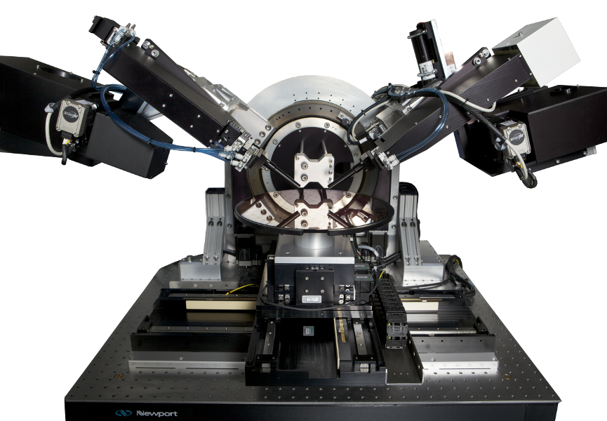
The µSE tool is designed to measure thin film thickness and optical properties inside a <50µm test pad on semiconductor product wafers. The applied measurement technique for obtaining these parameters in a high accuracy and repeatable way is spectroscopic ellipsometry. The μSE tool uses optimized spectroscopic ellipsometer (SE) arms and optics for the measurement inside small boxes of patterned Si wafers.
Ellipsometry measures the phase of the reflected light from the sample, therefore it is relatively insensitive for intensity fluctuations. The raw measurement data represent the complex information from the layer stack which then need to be modeled optically. The measurement results are obtained through numerical regression process of the model data to the raw measurement spectrum.
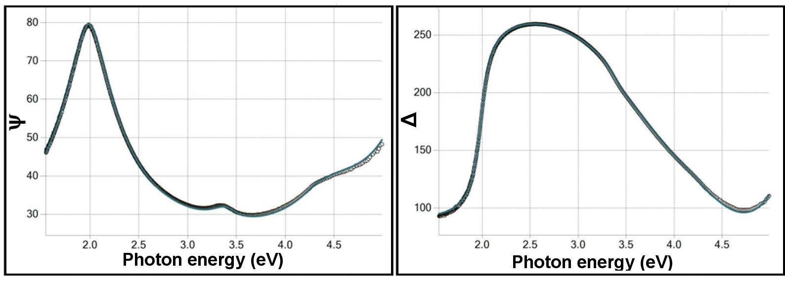
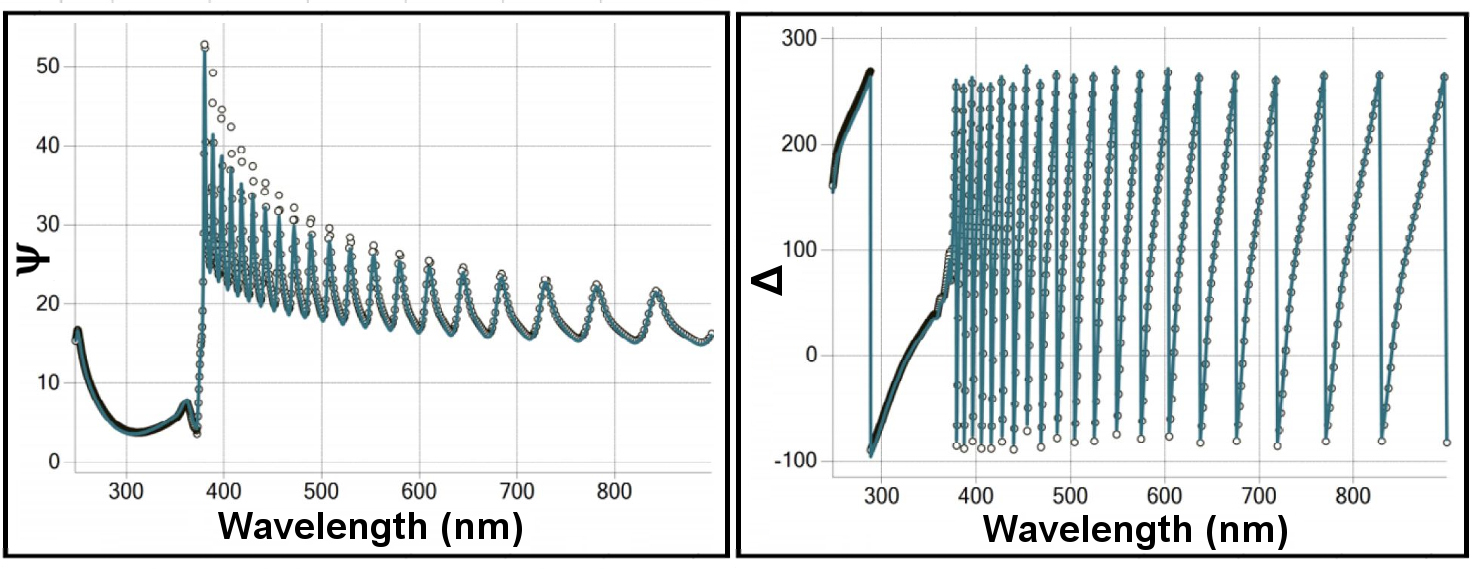
TYPICAL SE REGRESSIONS:
FEATURES
- Non-destructive optical technique, based on measurement of the change of the polarisation state of light after reflection at non normal incidence on the surface to study.
- It is a higly sensitive even for layer thickness below 5 nm
- Extremely versatile technique: it gives acccess to numerous parameters which characterize multilayer structures (eg. layer thickness, refractive index, absorption, porosity).
Product Line
SE
Refractive optical design in compact realization: short optical path inside the measurement arms (reduced alignment artifact errors). Active temperature control: stabilized environment for system reli-ability enhancement. Uniqe patented high brightness light source for outstanding SNR. CCD detector array (spectrum is taken simultaneously at different wavelengths).
Products

SE-2100
Printed Electronics. Optical & Electrical Metrology. Thin Film Coating characterization. Layer Thickness control.
Features and System specification:
- Capable for Fast and accurate measurement on square samples up to 350x450 mm or wafers up to 300 mm
- Special design of the chuck to hold Flexible Sample
- Active Vibration damping
- High-resolution mapping stage
- Fast Omron autofocus
- Vertical camera for samples visualisation & Pattern recognition
- Joystick to move the sample easily
- CE and SEMI standards compliant
Components & Options:
- Spectroscopic Ellipsometer:
- Fast acquisition directly on the foil
- Measurement Spot adapted for Plastic substrate
- Spectroscopic Reflectometer:
- For reflection and transmission of the films
- Non-contact Sheet resistance:
- Fast and accurate Sheet resistance by Eddy Current
- For Transparent electrode and Metal
- Other measurement technique like Raman, Lifetime...etc
Applications:
- Display: TFT, OLED on Glass or Flexible substrate
- Lighting: New OLED Lighting application. White OLED
- Printed Electronics: Any process on flexible substrate (transistor, sensors, etc.)
- Photovoltaics: Small Thin Films PV panels, TCO panels