


Application
THIN FILM APPLICATIONS
In order to keep the thin film solar cell production stable, the adequate control of the layer deposition and treatment processes is crucial. Semilab offers several metrology solutions for the characterization of electrical and optical properties of the thin layers.
Our special design Four-Point-Probe and Eddy Current sensors provide accurate measurement of the sheet resistance of thin semiconductor, TCO or even metal layers in the total range of interest.
Using Semilab’s Spectroscopic Ellipsometry and Spectroscopic Haze and Reflectance techniques the complete characterization of the layer thickness and other optical parameters can be accomplished even on multilayer structures.
.png)
Technology
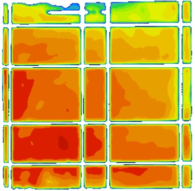
TCO SHEET RESISTANCE
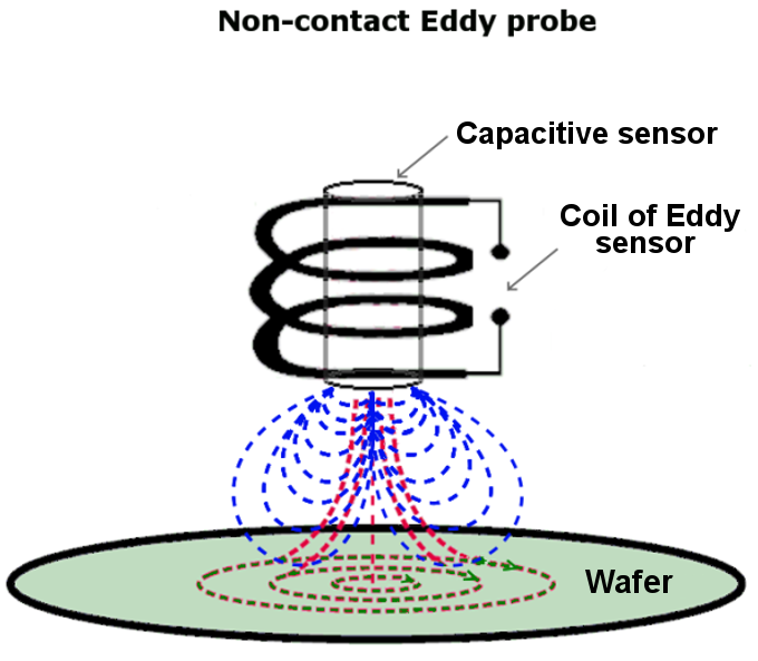
Sheet resistance measurement of thin films can be realized with help of non-contact, non-destructive Eddy current technique. Eddy current measurement is based on flow of AC current in a coil. Generated magnetic field induces circulating (Eddy) currents in the sample. The Eddy current measurement actually serves for obtaining of the electrical loss in the material. The measuring head moves above the sample in constant height, which is ensured by built-in distance sensor (based on capacitance measurement), while both of the sensors measures in the same spot. Because the measured signal depends on sample sheet resistance, and distance between the probe and sample, the true sheet resistance values can be obtained from the distance value and the Eddy signal.
The Eddy current is higher in good conducting material compared to less conductive ones.
FEATURES
- Non-contact, non-destructive method
Product Line
WT
The WT product line is a powerful measurement platform for performing many different semiconductor material characterization measurements. The base system includes all the overhead functions necessary to perform characterization measurements, including power supplies, computer and operating software, XY measurement stage, etc. The WT-2000 is typically used to make maps, where the wafer is scanned at a programmable raster. Each system is configured to the user’s requirements by adding treatment and measurement capabilities.
Products

WT-2000
The WT-2000 is a tabletop tool, suggested for mid-range fabs and laboratories.
Features and System Specifications:
- Wafer size: up to 300 mm with bare or dielectric coated surface
- Wafer handling: manual or Semilab-made indexer
- Loading options:
- 100-200 mm cassette indexer
- 300 mm 13 slot cassette indexer, including open cassettes for 100-300 mm wafers
- 300 mm 25 slot cassette indexer, including FOUP, FOSB, and open cassettes for 100-300 mm wafers
- Objectives of detection:
- Impurities due to heavy metal and transition metal contamination
- Crystal defects
- Optional iron concentration determination both in CZ and FZ wafers
- No wafer thickness limitation
- Fast measurement speed
- High lateral resolution
- Required surface passivation: thermal oxide, chemical passivation or corona charging
Each system can be configured based on the user’s requirements by adding measurement capabilities and automation capabilities described below.
Measurement capabilities:
- µ-PCD for measuring carrier lifetime
- SPV for measuring diffusion length
- JPV for measuring ion implants
- Eddy current measurement of sheet resistance
Request Info