


Application
THIN FILM APPLICATIONS
In order to keep the thin film solar cell production stable, the adequate control of the layer deposition and treatment processes is crucial. Semilab offers several metrology solutions for the characterization of electrical and optical properties of the thin layers.
Our special design Four-Point-Probe and Eddy Current sensors provide accurate measurement of the sheet resistance of thin semiconductor, TCO or even metal layers in the total range of interest.
Using Semilab’s Spectroscopic Ellipsometry and Spectroscopic Haze and Reflectance techniques the complete characterization of the layer thickness and other optical parameters can be accomplished even on multilayer structures.
.png)
Technology
SPECTROSCOPIC ELLIPSOMETRY (LTPS)
The Ellipsometry is an absolute, optical measurement technique, which measures the change of polarization of light, during passing through a medium. The phase of a polarized light exhibit distortion due to the layer structure during reflection, which enables us to extract material properties of the medium in this structure.
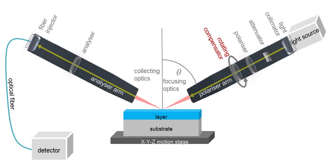
The distorted polarization can be determined by several method in which different optical components modulates the light polarization. Semilab is using the most advanced rotating compensator layout, where a high-end, broadband compensator introduce variable phase shift according to rotation angle in order to determine the ellipsometric components spectrally.
As ellipsometry is an indirect metrology, modelling and parameter fitting for the actual structure is necessary in order to extract the thickness and the refractive indices values. Semilab's Spectroscopic Ellipsometry Analyzer (SEA) software provides wide ranges of methods to build model for the actual structures and powerful algorithms fit the model parameters in order to obtain the values in interest.
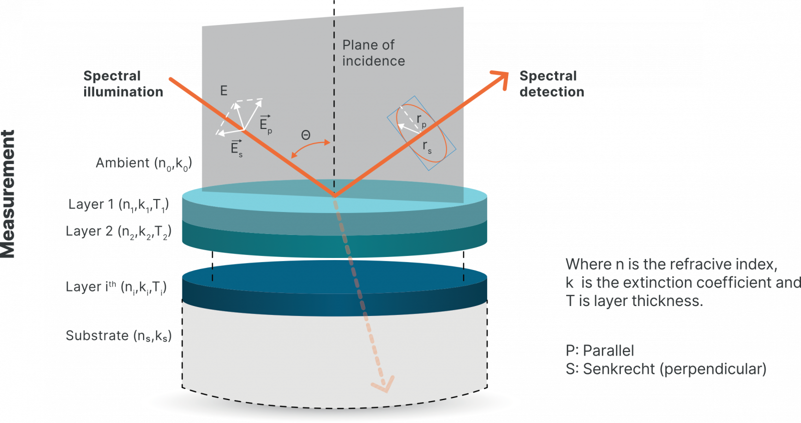
The Spectroscopic Ellipsometry measurement method has many advantages. First of all, it is an optical technique, so it is non-contact and non-destructive. It measures the layer thickness and optical functions of each layers in a multilayer structure. It has high sensitivity, because it is based on measuring the phase shift of a light beam travelling through a layer structure, and phase angle measurement does not depend on the absolute intensity of light. Using white light sources and monochromators, spectral information can be obtained about the sample.
Ellipsometry measures the ratio of the complex Fresnel reflection coefficients. As this is a complex number, it can be divided to an amplitude term, and a phase shift term, which correspond to the ellipsometric angles, Ψ and Δ. These parameters contain the physical properties of the layer structure, such as the layer thickness and refractive index. As this is a transcendental and highly nonlinear equation, it needs to be solved by numerical methods, on a model-based approach. During this procedure, the layer structure is considered with thickness and optical functions in the model. The relative phase shift is calculated and compared to measured quantities during a numerical regression procedure.
FEATURES
Non-contact and non-destructive optical measurements can be performed on:
- substrates
- single layer
- multi-layer samples
Obtained parameters: thin film thickness and optical properties
Covers a very broad of applications from semiconductor, organic, optics, bio, photovoltaics, laser diode, lighting, porous layer….
Measurement modes:
- Spectroscopic Ellipsometry for thin film thickness and optical functions, including complex multilayer structures
- Generalized Ellipsometry for Anisotropic materials
- Transmission Ellipsometry for transparent substrates
- Scatterometry vs. wavelength and angle of incidence
- Mueller Matrix (11 or 16 elements) uniquely offered in combination with Scatterometry for 3D anisotropic materials
- Jones Matrix for simple anisotropic materials
- Reflectance & Transmittance vs. wavelength and incidence angle
- Polarimetry
- Porosimetry: Measurements of pore size and porosity in thin films
- In-situ measurement mode for real time control during deposition or etch process
Product Line
FPT
FPT- series are dedicated for flat panel testing and characterization. The products are designed to characterize LCD and AMOLED TFT panels up to GEN 8.5. It is capable to combine several measurement probes into one platform, providing high precision measurements over the entire surface of flat panels with high accuracy and fast motorization stage and weight capacity.
Products

FPT
FPT can be equipped with:
- Spectroscopic ellipsometry
- Spectroscopic reflectometry
- Imaging Spectroscopic reflectometry
- Line mura detection - Chip quality
- Microwave Photoconductive Response - Chip Quality
- Four point probe & six point probe
- Contact angle measurement
- Raman crystallinity
Optical thickness and refractive index of multilayered oxide and semiconductor structures can be determined by spectroscopic ellipsometery at different process steps. The quality of the ELA process can also be monitored by measuring crystallinity, u-PCR and line mura density. Contact angle, stress and resistivity measurements are also available.
The hardware and software are fully controlled by SEMILAB from the design to the integrated software communication with the fab.
Request Info