


Application
CONTAMINATION MONITORING
Semilab’s suite of non-contact metrologies lead the IC industry for in-line detection of ultra-low metallic contamination. Semilab offers full wafer imaging solutions, ranging from the high throughput Photoluminescence Imaging technique (PLI) to more well-established lifetime-based methods, including Suface PhotoVoltage (SPV) and microwave Photoconductance Decay (µ-PCD). The flagship digital SPV technology (FAaST system) is industry standard that leads the world in bulk Fe detection.
There is no disputing the detrimental effect of metallic contamination on the integrity of the critical gate oxide used in integrated circuits. During high temperature processing, contamination in the silicon wafer often precipitates as a defect at the Si/Dielectric interface or segregates to the dielectric – in either case it has the potential to cause premature device failure and a reduction in product yield. The probability of metallic contamination impacting yield is a function of the chip size (e.g. technology node/critical dimension) and the defect density (e.g. the amount of contamination), such that as device dimension decrease, maintaining yield requires a corresponding reduction in contamination. Figure 1 clearly demonstrates the reality of this relationship over the past 25 years, during which time the IC industry has experienced a more than 3 orders of magnitude reduction in typical background Fe concentration observed in new fabs. More importantly the near term projection, where another order of magnitude reduction is needed to meet the requirements of the state-of-the-art Si IC manufacturing, with white pixel reduction in CMOS image sensors being a major stimulus for this effort.
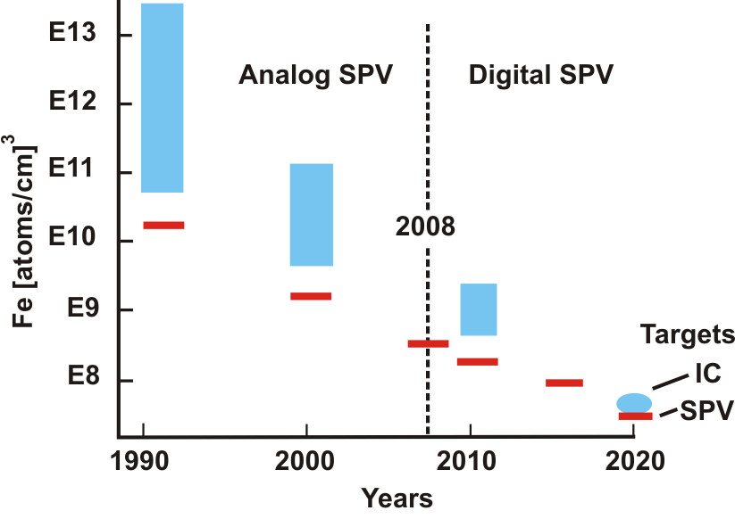
Figure 1. Typical background Fe concentration in new IC Fablines (blue) and the state-of-the-art SPV detection limit (red)
Technology
MINORITY CARRIER DIFFUSION LENGTH MEASUREMENT
Semilab SDI FAaST systems represent state-of-the-art non-contact electrical metrology used in manufacturing control and the development of semiconductor devices and materials. Employing non-contact surface potential probing techniques combined with illumination and/or non-invasive surface charging, these powerful techniques can measure a wide range of parameters characterizing semiconductor wafers, dielectrics and interfaces with astounding precision, while saving cost and time involved in fabricating dedicated test devices.
Due to „historical” reasons, SPV measurement is available in different system platforms. The surprisingly compact designed SPV sensor, integrated into WT-2000 multi-metrology platform contributes to the complete analysis of the electrical quality of the silicon wafers.
Semilab SDI's patented digital SPV technique - in FAaST systems - is the established world-leader for non-contact, non-destructive measurements of heavy metal contamination in silicon. SPV gives extremely fast, reliable measurements of minority carrier diffusion length, at low injection level. Together with proprietary activation techniques, it allows for identification of Cu and Fe contamination with unsurpassed sensitivity.
The small signal ac-surface photovoltage (SPV) minority carrier diffusion length measurement is an important diagnostic method used for monitoring iron contamination and micro defects in silicon wafers. It is used for evaluation of crystal growth, ingot to wafer processing and wafer cleaning. It is also used in IC fabs for monitoring iron contamination during key wafer processing steps and for requalification of processing tools after repair or maintenance.
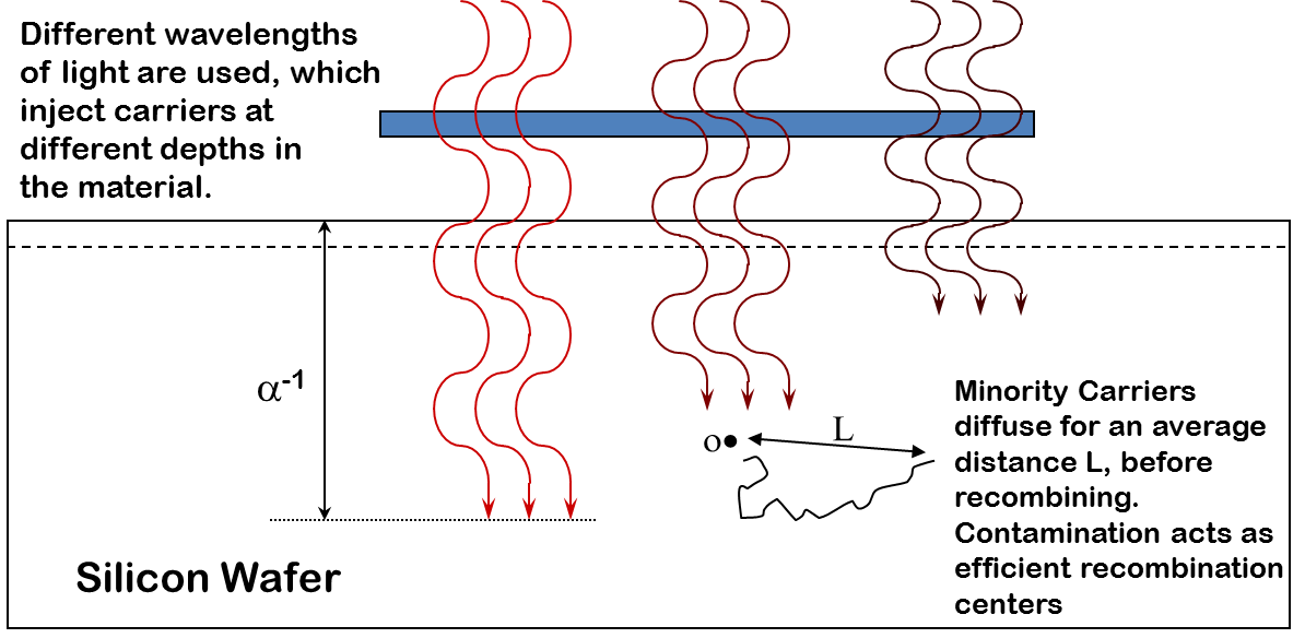
Figure 4. SPV illumination for minority carrier injection and subsequent carrier diffusion.
In ac-SPV metrology, multi-wavelength light, lK , generates excess minority carriers with different concentration profiles beneath the surface as determined by the light penetration depths z K (lK ). The excess carriers recombine and redistribute due to diffusion. The final profile is determined by z and by the minority carrier diffusion length, L = (Dtb)1/2 , where D is the diffusivity and tb is the bulk recombination lifetime. Sensitivity to iron and other recombination centers originates from tb and translates to the diffusion length in such a way that L-2 is a sum of factors proportional to concentrations of the individual recombination centers. Therefore, contamination monitoring is performed by measuring L. Individual contributions of different contaminants like Fe, Cu, and other recombination centers are obtained by manipulation of L-2 measured before and after wafer treatments that selectively change the recombination activity of individual contaminants. Such treatments are known for Fe and Cu and they involve strong illumination and/or thermal treatment.
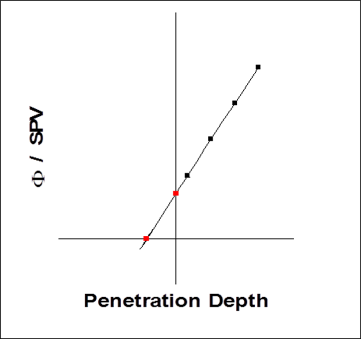 Figure 5. Extraction of diffusion length value (L), from measured SPV signal vs light penetration depth
FEATURES
- Separation and quantitative measurements of:
- Fe concentration; detection limit 108 cm-3
- Cu concentration – from activation of Cu=Cu pairs
- Co concentration (in engineering mode)
- Low carrier injection, constant photon flux approach
- Temperature stabilized digital illuminator (LED)
- In situ diffusion length calibration reference
- Variable intensity digital detrapper
- Ability to measure on bare and oxidized Si wafers
- The only system in the world, which can truly separate bulk minority carrier diffusion length, from front and back surface recombination
- Unique L0 steady state diffusion length measurement
- Precise measurement of steady state minority carrier diffusion lengths up to 3× wafer thickness
- Production-friendly non-contact, non-destructive, including full Si coverage without edge exclusion
- In situ wafer preparation and Fe-B recovery (annealing station)
- Production proven tool to tool matching
Product Line
WT, FAaST
The WT product line is a powerful tabletop measurement platform for performing many different semiconductor material characterization measurements. The base system includes all the overhead functions necessary to perform characterization measurements, including power supplies, computer and operating software, X-Y measurement stage and so on. It is typically used to make maps, where the wafer is scanned at a programmable raster.
FAaST metrology includes best in the world Semilab SDI unique capabilities:
- The Digital Surface PhotoVoltage (DSPV) measurement of minority carrier diffusion length with unmatched sensitivity for Fe detection in Si wafers below 1E8 atoms/cm3.
- Corona-Kelvin characterization of dielectrics and interfaces with capability for pattern wafer measurement and micro-scale scribe-line (SL) measurement using micro-corona and Kelvin Probe Force Microscopy (KPFM).
- Wafer mapping is available for all measured parameters and especially high-throughput mapping of non-visual defects, including electrical charge defects caused by plasma etching, ion implantation, or mobile ion contamination.
Semilab SDI FAaST systems offer:
- Flexible configurations that can be customized to suit individual customer needs.
- Platforms, range from a fully automated dual 300 mm loadport system configured with all measurement options and capable to meet the 300 mm Semi requirements of modern IC Fabs to manual load systems configured with a single measurement technology that can measure samples as small as approximately 20 mm × 20 mm making them well-suited for the university or laboratory environment.
Products

FAaST 310/210 SPV
The FAaST 310/210 SPV systems provide fast, full wafer contamination imaging in a design suitable for R&D and low-volume manufacturing environments.
Features and System specifications:
- Manual wafer loading, including cassette placement station and vacuum wand
- Automatic full wafer FAST mapping of diffusion length, Iron, and Other Recombination Centers (Nr)
- FAaST software package, including measurement, recipe writing and data viewing applications
- Configurable for 50 mm to 300 mm wafers, with options available for multiple wafer sizes
- Step down power transformer with flexible compatibility
- Additional available options include: Automatic data upload and/or data export, Seismic brackets

FAaST 330/230 DSPV
The FAaST 330/230 DSPV systems are designed to provide world-leading, non-contact fast in-line monitoring of heavy metal contamination, including sub 108 atoms/cm-3 Fe detection, with automated wafer handling that is suitable for the medium to high-volume manufacturing environment.
Features and System specifications:
- Automatic robotic wafer handling
- Single open-cassette wafer loading station with configurable options including SMIF / FOUP Loadport / Versaport
- Automatic full wafer FAST mapping of diffusion length, Iron, and Other Recombination Centers (Nr)
- Option for advanced digital SPV functions, including Backsurface Recombination (Sb), Steady State Diffusion Length (L0), and Copper measurements
- FAaST software package, including measurement, recipe writing and data viewing applications
- Configurable for 100 mm to 300 mm wafers, with options available for multiple wafer size
- Line conditioner with flexible compatibility
- Compatible for configuration with other Semilab SDI FAaST tool measurement technologies
- Additional available options include: Minienvironment, wafer edge-grip handling, wafer flipper for automatic backsurface measurement, 300 mm Semi-compliant automation, Seismic brackets, wafer OCR, RFID, cassette barcode reader

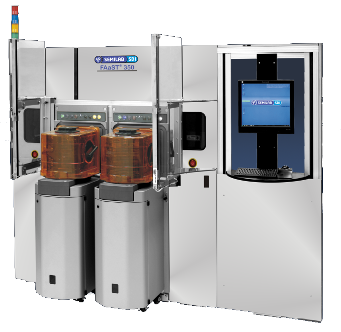
FAaST 350 DSPV
The FAaST 350 DSPV system is the flagship platform designed to provide world-leading, non-contact fast monitoring of heavy metal contamination, including sub 108 atoms/cm-3 Fe detection, with automated wafer handling from dual FOUP loadport loading stations fully capable of supporting the most demanding high-volume manufacturing environment.
Features and System specifications:
- Automatic robotic wafer handling
- Dual FOUP loadport; optional configuration with single loadport or including Versaport
- Automatic full wafer FAST mapping of diffusion length, Iron, and Other Recombination Centers (Nr)
- Option for advanced digital SPV functions, including Backsurface Recombination (Sb), Steady State Diffusion Length (L0), and Copper measurements
- FAaST software package, including measurement, recipe writing and data viewing applications
- Default configuration for 300 mm wafers with option for 200 mm / 300 mm bridge configuration
- Line conditioner with flexible compatibility
- Compatible for configuration with other Semilab SDI FAaST tool measurement technologies
- Additional available options include: Minienvironment, wafer edge-grip handling, wafer flipper for automatic backsurface measurement, 300 mm Semi-compliant automation, Seismic brackets, wafer OCR, RFID, cassette barcode reader

WT-2000
The WT-2000 is a tabletop tool, suggested for mid-range fabs and laboratories.
Features and System Specifications:
- Wafer size: up to 300 mm with bare or dielectric coated surface
- Wafer handling: manual or Semilab-made indexer
- Loading options:
- 100-200 mm cassette indexer
- 300 mm 13 slot cassette indexer, including open cassettes for 100-300 mm wafers
- 300 mm 25 slot cassette indexer, including FOUP, FOSB, and open cassettes for 100-300 mm wafers
- Objectives of detection:
- Impurities due to heavy metal and transition metal contamination
- Crystal defects
- Optional iron concentration determination both in CZ and FZ wafers
- No wafer thickness limitation
- Fast measurement speed
- High lateral resolution
- Required surface passivation: thermal oxide, chemical passivation or corona charging
Each system can be configured based on the user’s requirements by adding measurement capabilities and automation capabilities described below.
Measurement capabilities:
- µ-PCD for measuring carrier lifetime
- SPV for measuring diffusion length
- JPV for measuring ion implants
- Eddy current measurement of sheet resistance
Request Info

WT-2000 / 2A
The WT-2000 is suggested for mid-range fabs and laboratories.
Features and System specifications:
- Wafer size: up to 300 mm with bare or dielectric coated surface
- Wafer handling: manual or Semilab-made indexer
- Loading options:
- 100-200 mm cassette indexer
- 300 mm 13 slot cassette indexer, including open cassettes for 100-300 mm wafers
- 300 mm 25 slot cassette indexer, including FOUP, FOSB, and open cassettes for 100-300 mm wafers
- Light sources: semiconductor lasers (SPV head with 4 or optional 8 lasers)
- Full mapping
- Point measurements at predefined points
- Sample resistivity: down to 0.01 Ωcm
- Optional bias light:
- High intensity IR LED
- 30 W halogen lamp
- Automatic Iron-Boron Dissociation Unit - for Iron concentration
- Specific measurement performance at specific, programmable locations
Each system can be configured based on the user’s requirements by adding measurement capabilities and automation capabilities described below.
Measurement capabilities:
- µ-PCD for measuring carrier lifetime
- SPV for measuring diffusion length
- VQ for oxide monitoring
- JPV for measuring ion implants
- Eddy current measurement of sheet resistance
Request Info