


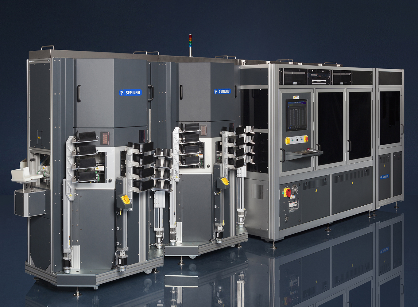
Application
SI WAFER SORTING
Sorter applications provide advanced multiparameter wafer inspection with integrated high speed sorting for quality control of production PV wafers. Owing to wide range automation module portfolio and flexible combined Semilab’s metrology modules, all customer can find perfect configuration what fulfil their production expectations.
Application area:
- Outgoing wafer inspection for wafer manufacturers
- Incoming as-cut wafer inspection for solar cell manufacturers
Sorter purpose
- Eliminating damaged wafers from further process
- Eliminating high thickness variation wafers (TTV, saw mark)
- Sorting of potentially weak wafers (microcracks) which could break in subsequent process steps
- Sorting based on resistivity, and lifetime values
- Sorting of wafers with dislocations, high contamination and vacancy density
- Wafer input: loading from cassettes or stack
- Wafer output: Sorting in different user-defined classes, collection in coin stacks
- High throughput
Technology
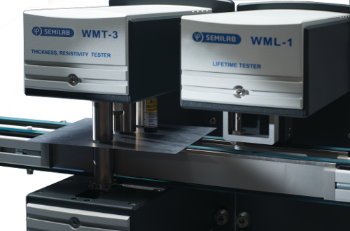
THICKNESS AND RESISTIVITY MEASUREMENT
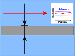
Thickness is a primary control parameter of silicon PV wafers. By filtering out wafers with non-standard thickness and shape, waste from wafer/cell breaking can be reduced.
Thickness of PV wafers is measured for two reasons:
- To insure specification. From the thickness measured in different points of the wafer, the following parameters can be calculated:
- Average thickness
- Total Thickness variation (TTV)
- Thickness Deviation
- To obtain resistivity value by using the Eddy current technique based on thickness information to report the bulk resistivity of the sample.
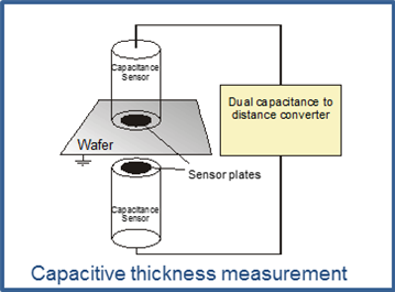
Thickness
WMT/WML uses capacitive probes to measure the distance from wafer surfaces. This way the result is independent on surface quality (reflection).
The capacitance depends on the distance between the probe and the sample:
C = Ɛ . (A/d)
where d is the probe-sample distance. From the measured capacitance the distance can be calculated, and the distances from both sides of the sample makes the thickness determination possible.
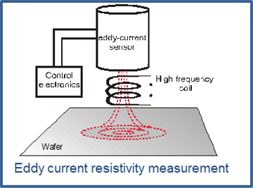
Resistivity
Resistivity measurement is based on non-contact Eddy current method
An AC current flows in a coil in close proximity to a conducting material. The magnetic field of the coil induces circulating (Eddy) currents in the sample. The Eddy current measurement is actually the measurement of the electrical loss in the material, which depends on the resistivity. The signal in the sensor is calibrated to samples certified with 4PP.
The tool measures line scans parallel to the belt direction:
- 6 saw mark line scans (3 on the top, 3 on the bottom)
- 3 thickness line scans
- 1 resistivity line scan
Position of the line scans: 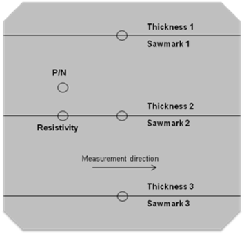
FEATURES
- Non-contact, non-destructive measurement for inline PV applications
- Every single wafer can be measured in production
- No wearing parts unlike 4PP
- Grain size independent resistivity measurement
Product Line
PVS
WMT/WLT inline tools allow non-contact, preparation free, high-speed thickness and bulk resistivity measurement of crystalline wafers. Robust design and easy integration makes it an obvious choice for wafer sorter applications to sort out of spec wafers. Special design of capacitive probes makes good accuracy even on non-grounded wafers such as in the case of belt transport. Unique design of resistivity sensor makes it independent of grain size variation.
Operating modes and configuration:
- WLT is operating in Stop & Go mode with 1 to 5 thickness sensor pairs and one resistivity sensor
- WMT can measure 1 to 3 line scans in on-the-fly mode with sensor pairs and one line resistivity
Products

PVS-5000
PVS-5000 is a high throughput, field proven PV Wafer Inspection and Sorting System.
It combines high reliability wafer handling with Semilab’s industry leading PV metrology, to provide a turnkey solution for sorting of incoming wafers. This is backed by direct expert support from the OEM metrology manufacturer, through our worldwide network of branch offices.
Loaders
- PVLS-5400 Automated stack loader with 3 position pick-and-place system. Up to 2400 pcs buffered wafer in 12 pcs carrier.
- PVLC-3600* Automated cassette loaders for 25/50/100 slot cassettes
- PVLC-3600-AL Fully automated production line loader for 100 slot cassettes
Metrologies
- PLI-101/3 Photoluminescence imaging
- WML-1 Minority carrier lifetime measurement
- SHP-200 2D measurement
- MCI-150 Micro crack inspection
- WSI-120 Surface chipping and contamination inspection
- TTR-300 Thickness, resistivity measurement
- TTR-300 Saw mark Inspection
Unloaders
- PVULS-5406T High speed stack unloader with 6 bin
- PVULS-5407T High speed multilevel stack unloader with 7 bin

PVS-6000
PVS-6000 is a High Speed, field proven PV Wafer Inspection and Sorting System with 5400 wafer per hour throughput. It combines high reliability wafer handling with Semilab’s industry leading PV metrology, to provide a turnkey solution for sorting of incoming wafers. This is backed by direct expert support from the OEM metrology manufacturer, through our worldwide network of branch offices.
Loaders:
- PVLS-5400 Automated stack loader with 3 position pick-and-place system. Up to 2400 pcs buffered wafer in 12 pcs carrier.
- PVLC-3600 Automated cassette loaders for 25/50/100 slot cassettes
- PVLC-3600-AL Fully automated production line loader for 100 slot cassettes
Metrologies:
- PLI-101/3 Photoluminescence imaging
- WML-1 Minority carrier lifetime measurement
- SHP-200 2D measurement
- MCI-150 Micro crack inspection
- WSI-120 Surface chipping and contamination inspection
- TTR-300 Thickness, resistivity measurement
- TTR-300 Sawmark Inspection
Unloaders:
- PVULS-5406T High speed stack unloader with 6 bin
- PVULS-5407T High speed multilevel stack unloader with 7 bin