


Application
PRINTED OLED SUB-PIXEL CHARACTERIZATION
Printing OLED is very attractive way for producing organic layer containing devices due to its low price and relatively easy technique. However, in many cases the uniformity of printed layers is much worse than the conventionally manufactured layers.
Semilab has developed a metrology which can determine the full thickness of OLED structure in one sub-pixel using a single measurement in a few seconds. The lateral resolution can be as high as 5 µm which allow to our customer to fine tune precisely the printing process.
![]()
Technology
IMAGING SPECTROSCOPIC REFLECTOMETRY
Imaging Spectroscopic Reflectometry is used for investigating high spatial resolution of small (typically 50x50 µm to 500x500 µm) areas. As a consequence, the two main applications are half-tone process control (where photoresist thickness characterization is possible down to 1 µm channel width) and printed OLED thickness map. By means of a high-brightness Xe-lamp as light source and high-precision monochromator fast and accurate measurement can be performed. The wavelength resolution is adjustable down to several nanometers and wavelength range can be chosen according to the thickness and optical properties of the measured layer.
The wide wavelength-range light source is filtered by a monochromator. The monochrome light reaches the sample and a 2D image is captured in the same time. This process is repeated for every selected wavelength which will result in a set of images, each represent the result at a given wavelength. Using these pictures the software calculates the reflectance spectra for each selected site.
Imaging Spectroscopic Ellipsometry requires very precise focusing which is done by a built-in focusing system utilizing a fast and precise piezoelectric motor.
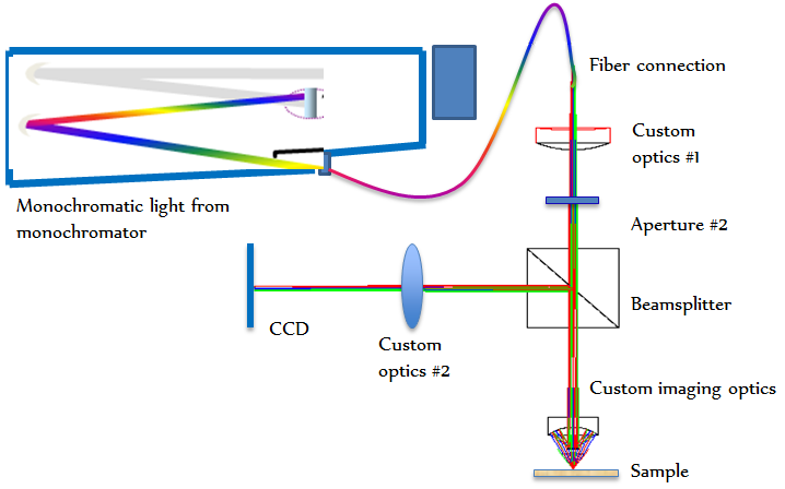
Imaging Spectroscopic Reflectometry uses the same analysis engine than Spectroscopic Reflectometry and Ellipsometry, Consequently the same optical model can be used for the same material even if being measured by two different metrologies. This makes us able to use refined optical models based on precise spectroscopic ellipsometry (which is needed for e.g. OLED samples).
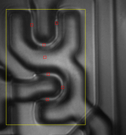
H / T Process Control
PR Thickness in channel
FEATURES
- High-brightness Xe-lamp for fast and accurate acquisition
- High spatial resolution
- Same analysis engine as Specotrscopic Ellipsometer and Spectropscopic Reflectometer is used
- Adjustable (by recipe) wavelength range and resolution
- Unlimited measurement points can be selected on the acquired image.
Product Line
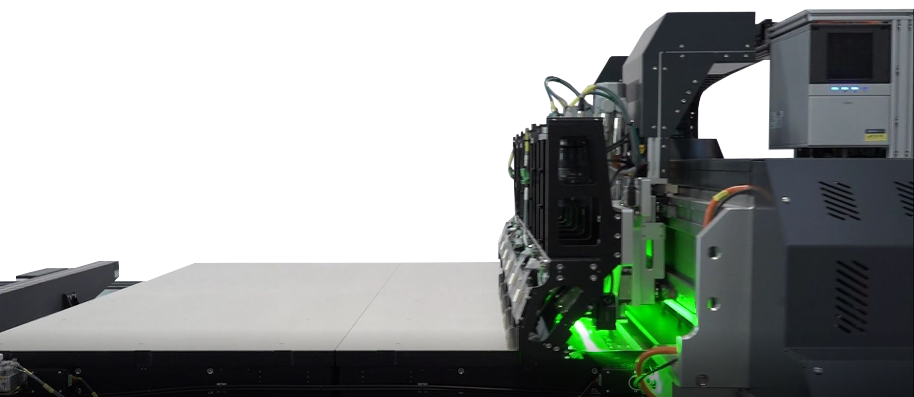
FPT
FPT- series are dedicated for flat panel testing and characterization. The products are designed to characterize LCD and AMOLED TFT panels up to GEN 8.5. It is capable to combine several measurement probes into one platform, providing high precision measurements over the entire surface of flat panels with high accuracy and fast motorization stage and weight capacity.
Products

FPT
FPT can be equipped with:
- Spectroscopic ellipsometry
- Spectroscopic reflectometry
- Imaging Spectroscopic reflectometry
- Line mura detection - Chip quality
- Microwave Photoconductive Response - Chip Quality
- Four point probe & six point probe
- Contact angle measurement
- Raman crystallinity
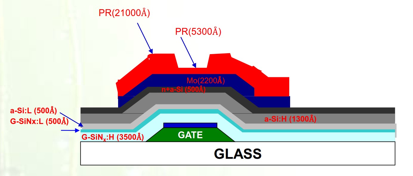
Optical thickness and refractive index of multilayered oxide and semiconductor structures can be determined by spectroscopic ellipsometery at different process steps. The quality of the ELA process can also be monitored by measuring crystallinity, u-PCR and line mura density. Contact angle, stress and resistivity measurements are also available.
The hardware and software are fully controlled by SEMILAB from the design to the integrated software communication with the fab.
Request Info