


Application
SHEET RESISTANCE MEASUREMENT
The combination of the ion implant process and the process to anneal implants is usually monitored by measuring the sheet resistance of the implanted layer. The sheet resistance varies with dose, energy, and the amount of implanted species that has become electrically active. It is the sheet resistance that ultimately determines the device performance. Thus, measuring sheet resistance is an excellent way to monitor everything associated with an implant process.
The basic idea of the JPV method is the light excitation of the np or pn layer structure, and the pick-up of the resulting junction photovoltage by a capacitive probe. The detected potential is determined by the sheet resistance of the implanted layer, capacitance of junction and resistance through over the diode.
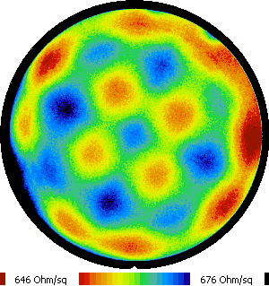
Figure 2. Sheet resistance measurement (lower range)
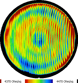
Figure 3. Sheet resistance measurement (higher range)
Semilab offers JPV technology to make non-contact, high resolution fast maps of sheet resistance.
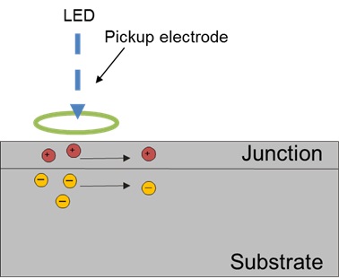
Figure 4. Measurement theory
MEASUREMENT THEORY:
The sample is illuminated by chopped LED light, which generates electrons and holes in the substrate layer. The generated charge carriers diffuse to the junction and the electric field located in the junction separates them. The result of the separation is the change in the junction voltage. This voltage change spread laterally in the implanted layer and the attenuation depends on the sheet resistance, junction capacitance, resistance of the junction and chopping frequency of the LED.
The potential change is detected by a capacitive sensor in order to evaluate the JPV signal, as a function of the frequency of the emitted light.
Based on the evaluation, the sheet resistance (Rs), capacitance of junction (Cd) and the resistance of the diode (Rd) can be calculated.
The junction leakage current is directly connected to the Rd by the following equation:
I_L=kt/q/R_d
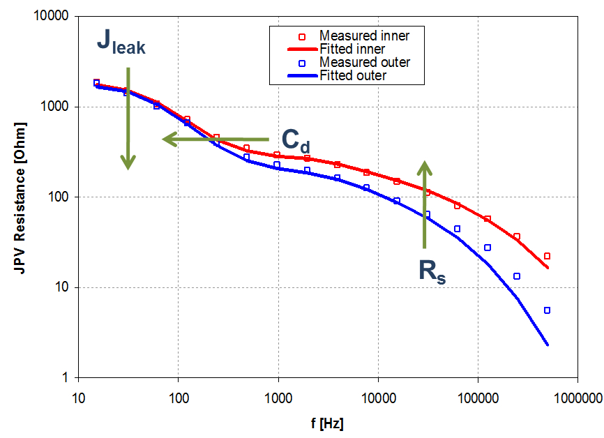
Figure 5. The detected potential is determined by Rs, Cd, Rd and frequency
Technology
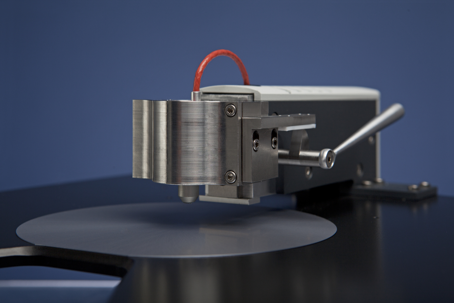
CONTACT SHEET RESISTANCE MEASUREMENT
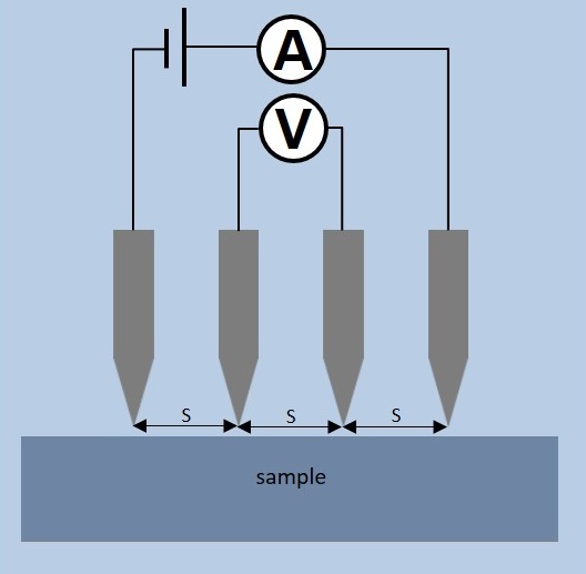
The four point probe (4PP) is a widely used contact technique for monitoring of doping density, resistivity or emitter sheet resistance values. The separation of voltage and current electrodes eliminates the effect of contact resistance from the measurement result. The used voltage is limited so in the high resistivity range the measurable current is getting very small which sets a limitation for the measurement. With our six pin probe (6PP) technique we overcome this problem by using two additional pins to suppress the measurement noise as much as possible..
METROLOGY OVERVIEW
The sample is contacted by four pins and a current generator leads a defined current through the sample via the outer pins. The two inner pins are used to measure the voltage between them. From these two parameters, the sample’s sheet resistance can be calculated. The space between the pins is equal (1mm for 4PP and 1.5mm for 6PP). The pin material is produced from tungsten carbide (4pp) and stainless steel (6pp). In case of 4pp the contact force and the curvature of the pins can be chosen as required for a given material. Periodical calibration isn’t necessary for this kind of measurement technique because it’s based upon self-calibration.
FEATURES
- Extended measurement range with 6PP up to 1TΩ/sq.
- Wide selection of pin’s curvature and probe force in order to get precise result with minor destruction.
Product Line
FPT
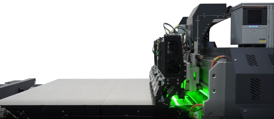
FPT- series are dedicated for flat panel testing and characterization. The products are designed to characterize LCD and AMOLED TFT panels up to GEN 8.5. It is capable to combine several measurement probes into one platform, providing high precision measurements over the entire surface of flat panels with high accuracy and fast motorization stage and weight capacity.
Products

FPT
FPT can be equipped with:
- Spectroscopic ellipsometry
- Spectroscopic reflectometry
- Imaging Spectroscopic reflectometry
- Line mura detection - Chip quality
- Microwave Photoconductive Response - Chip Quality
- Four point probe & six point probe
- Contact angle measurement
- Raman crystallinity
Optical thickness and refractive index of multilayered oxide and semiconductor structures can be determined by spectroscopic ellipsometery at different process steps. The quality of the ELA process can also be monitored by measuring crystallinity, u-PCR and line mura density. Contact angle, stress and resistivity measurements are also available.
The hardware and software are fully controlled by SEMILAB from the design to the integrated software communication with the fab.
Request Info