Application
LABORATORY APPLICATIONS
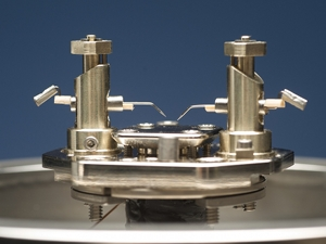
Troubleshooting manufacturing process needs more comprehensive analysis of the wafers in different process steps. Often these tests are out of scope of in-line and offline process control tools. For this purpose Semilab can offer state-of-the art laboratory tools with multiple capabilities.
These advanced metrology tools can be effectively used in the research and development field to introduce new methods and techniques for high efficiency solar cell production.
Semilab is open for cooperation with customers to improve the tool performance and introduce new applications to cover future metrology needs.
The measurement tools were designed to achieve good tool performance, user-friendly operation and low cost of ownership.
The applications include the following:
- Wafer contamination characterization
- Analytical contamination detection in wafers
- Measurement of electrical parameters in different manufacturing stages
- Optical characterization of deposited layer parameters
- Electrical characterization of deposited dielectric layer parameters
- Measuring surface passivation efficiency and homogeneity
- Testing accelerated light-induced degradation (LID) and potential-induced degradation (PID) of solar cells