


Application
LABORATORY APPLICATIONS
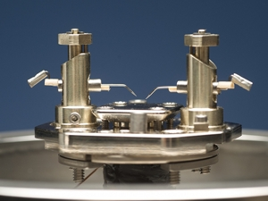
Troubleshooting manufacturing process needs more comprehensive analysis of the wafers in different process steps. Often these tests are out of scope of in-line and offline process control tools. For this purpose Semilab can offer state-of-the art laboratory tools with multiple capabilities.
These advanced metrology tools can be effectively used in the research and development field to introduce new methods and techniques for high efficiency solar cell production.
Semilab is open for cooperation with customers to improve the tool performance and introduce new applications to cover future metrology needs.
The measurement tools were designed to achieve good tool performance, user-friendly operation and low cost of ownership.
The applications include the following:
- Wafer contamination characterization
- Analytical contamination detection in wafers
- Measurement of electrical parameters in different manufacturing stages
- Optical characterization of deposited layer parameters
- Electrical characterization of deposited dielectric layer parameters
- Measuring surface passivation efficiency and homogeneity
- Testing accelerated light-induced degradation (LID) and potential-induced degradation (PID) of solar cells
Technology
LIGHT BEAM INDUCED CURRENT
The quantum efficiency of the solar cell in the photovoltaic industry is one of the most important indicator. It is given as the ratio of the induced electron current (Ielectron) of solar cell and the incident photon current (Iphoton) and depends on the light wavelength and the number of solar cell properties. There are two different quantum efficiency definitions:
- External quantum efficiency: the Iphoton is not corrected by the reflection of the induced light on the wafer surface
- Internal quantum efficiency (IQE): the Iphoton is corrected by the reflection
Quantum efficiency of solar cell is limited by different losses:
- Optical
- Electrical
- Ohmic
- Recombination - carrier lifetime related
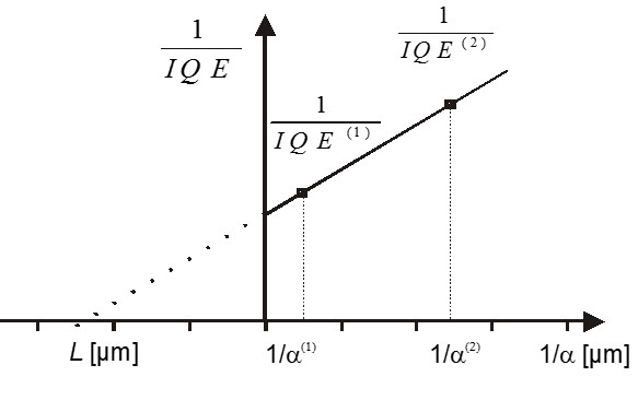
Reliable method of obtaining of IQE value is Light Beam Induced Current (LBIC) method of measurement.
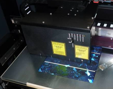
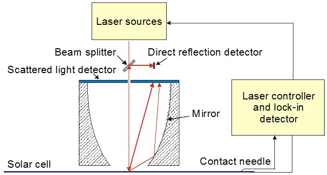
LBIC technology is based on the electrical current measurement. Laser beam is shined on the sample in one point and creates electrical current which is measured by the tool and represents the short circuit current (ISC) at the given illumination. The reflection (R) of the multiple laser source is sensed by reflection detector. From the ISC and reflection values can be determined the IQE. Using multiple wavelengths, the diffusion length (L) can be measured. The theory is similar to the SPV technique:
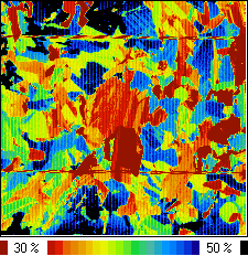
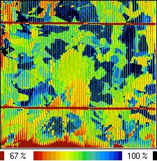
LBIC application examples:
| LBIC | Reflectance | IQE | |
|---|---|---|---|
| 980 nm IR laser: | 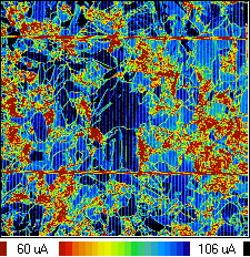 |
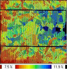 |
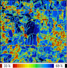 |
| 405 nnm Blue laser: | 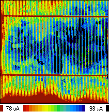 |
 |
 |
FEATURES
- Multiple wavelength laser capability
- Adjustable light intensity
- Separated direct and scattered reflection measurement
- Reflected light is detected up to an angle of 60o
- Parameters Measured:
- Short circuit current
- External quantum efficiency
- Reflectance (optional)
- Internal quantum efficiency (needs Reflectance option)
- Minority carrier diffusion length (optional)
Product Line
WT, PV
The WT product line is a powerful measurement platform for performing many different semiconductor material characterization measurements. The base system includes all the overhead functions necessary to perform characterization measurements, including power supplies, computer and operating software, XY measurement stage, etc.
The WT-2000 is typically used to make maps, where the wafer is scanned at a programmable raster. Each system is configured to the user’s requirements by adding treatment and measurement capabilities.
The world’s most powerful PV metrology system. Unparalleled mapping, precision, repeatability and tool matching
Products

PV-2000A
Features and System specifications:
It is a new integrated platform with the following capabilities:
- SPV Diffusion Length
- Discrete ites and mapping of incoming and processed wafers to final cells.
- UV/Blue SPV ratio for surface passivation (arb. units)
- Monitorable parameters:
- Diffusion length (L)
- Fe contamination (Fe)
- Other Recomb. Centers (NR)
- LID Defect Contamination
- Noncontact C-V profiling
- Time resolved approach with leakage correction
- Monitorable parameters:
- Flatband Voltage (Vfb)
- Oxide Total Charge (Qtot)
- Interface Trapped Charge (Qit)
- Interface Trap Density (Dit)
- Dielectric Capacitance (CD) and thickness (CET),
- Dielectric Leakage and PID testing 3 to 1000 nm planar and textured films
- Accelerated LID testing
- Temperature stages (20-220°C), 2 illumination stations (halogen and flash); robotic handling: activates/deactivates iron and/or boron-oxygen
- LID defects in minutes
- ALID is sequenced with SPV for Fe and LID defect mapping in short time
- Applicable to wafers and solar cells
- QSS-μPCD
- Discrete sites and mapping of incoming and processed wafers
- PCD laser wavelength: 904 nm
- Monitorable parameters:
- Decay lifetime (τ eff.d)
- Steady-state lifetime (τ eff.ss)
- Injection level (Δn)
- Effective surface recombination (Seff)
- QSS light intensity: 0.005 to 30 Suns
- Emitter Saturation Current (J0)
- Implied Voc
- Light Beam Induced Current (LBIC)
- Mapping of solar cells 1 to 4 lasers
- Measurement parameters: Current; Diffusion Length; Reflectance; Internal Quantum Efficiency (IQE)
- Reflectance measurement and IQE mapping
Other testing capabilities:
- SPV Surface Lifetime
- SPV Mapping of Rshunt and Voc
- Noncontact Suns-Voc
- Wafer Thickness Measurement

WT-2000PVN
The WT-2000PVN is a table top measurement system, capable of performing a variety of measurements on PV cells, wafers, and blocks. The base system includes the overhead functions, and you configure the measurement capabilities to match your specific needs, by selecting from the options below.
The WT-2000PVN can measure blocks and ingots, as well as wafers and cells. For measuring wafers and cells, people typically produce maps. When measuring blocks or ingots, people often produce only line scans, to save time, WT-2000PVN can do both.
Most producers of PV cells own a WT-2000PVN. It is extremely useful for:
- Engineering development and characterization
- Batch testing of production
- Comprehensive troubleshooting of production problems
Measurement techniques that can be integrated in WT-2000PVN:
- µ-PCD / carrier lifetime
- Measured parameter: carrier lifetime
- High resolution mapping and discrete point measurements
- SHR / sheet resistance
- Measured parameter: emitter sheet resistance
- Mapping and discrete point measurements
- LBIC / photovoltaic response, quantum efficiency, diffusion length
- High resolution mapping with 1 to 4 lasers
- Measured parameters:
Short circuit current
Direct and scattered reflectance
IQE and EQE
Diffusion length
- Eddy current resistivity
- Non-contact resistivity mapping
- Different resistivity range probes
- Bias light to µ-PCD