


Application
IGZO ELECTRICAL CHARACTERIZATION
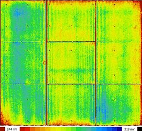
IGZO is one of the state-of-the-art active layer for display industry. However even today the fine tuning of the process requires very precise measurements in order to maintain the best layer properties.
Using Semilab’s µ-PCR and contact sheet resistance measurement one can map the panel with a reasonable speed which can show the improper settings of the layer deposition and set up the possibilities for further optimization
µ-PCR can determine a parameter (amplitude) which related to the device mobility, moreover other layer quality parameters (calculated from the microwave response decay curve) can be calculated as well.
Technology
MICROWAVE PHOTOCONDUCTIVE RESPONSE
µ-PCD / µ-PCR FOR FLAT PANEL INDUSTRY
For a better throughput of fabrication, TFT industry needs characterization methods for process optimization. By means of the Microwave Photoconductive Decay (µ-PCD) and Microwave Photoconductive Response (µ-PCR) metrology, the electrical properties of the active layer can be tested right after layer deposition or later throughout the process, before forming the devices themselves. This early-stage, non-contact, non-destructive characterization method can be utilized either in case of InGaZnO (IGZO) and Low-temperature Poly-Silicon (LTPS)-based TFT panel processes.
METROLOGY OVERVIEW:
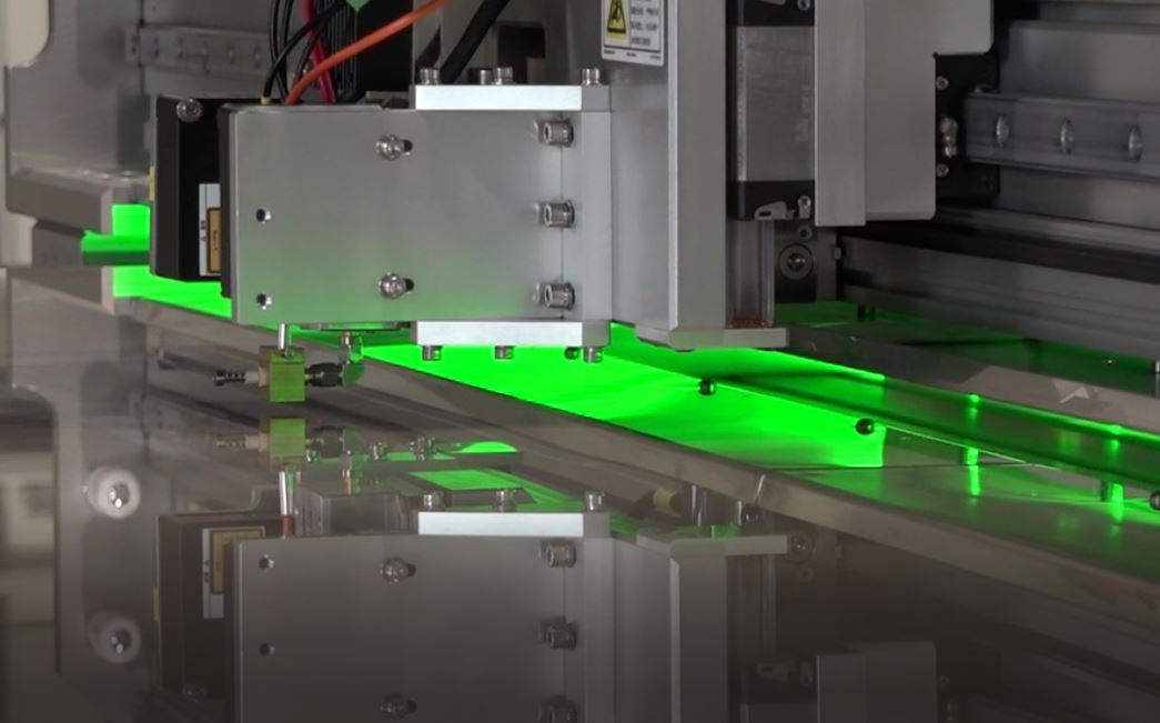
Excitation by UV-laser
Thin films of IGZO and LTPS – i.e. the active layer of a TFT – can be characterized by monitoring the excited charge carrier behavior in these materials. By exciting the charge carriers, the recombination behavior monitoring can provide a fingerprint of the layer electrical properties.
A pulsed UV-laser (349 nm) is used for excitation: the pulse creates electron-hole pairs in the material. The recombination can happen through different physical phenomena, which are typically trap-assisted or Auger-processes, etc. By measuring the recombination of the charge carriers, we can draw conclusions to physical properties of the material, thus the electrical quality and homogeneity can be evaluated.
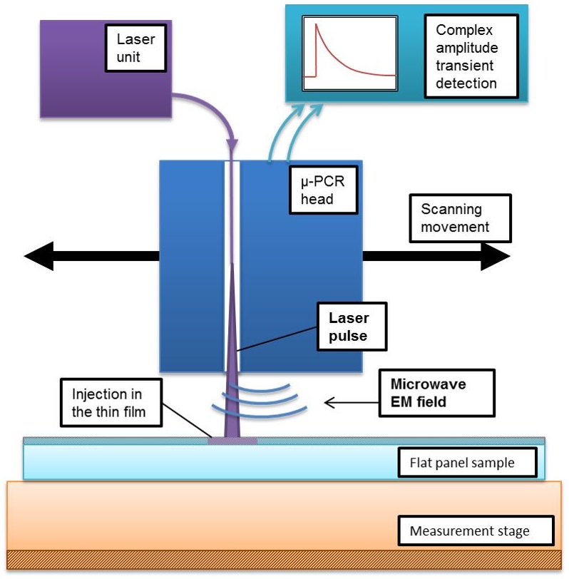
Microwave detection of transient behavior
The charge carrier recombination can be detected by means a non-contact microwave metrology system. A tunable ~22-26 GHz microwave field is radiated onto the sample surface using a compact waveguide antenna. Tuning can compensate sample effects and is done automatically. The source of the field is a Voltage Controlled Oscillator (VCO). Microwave local signal and reflection from the sample is measured.
The laser excitation changes the free charge carrier concentration in the sample, thus microwave reflection will then suffer great change. As the charge carriers recombine through different physical phenomena, a transient decay can be measured, which in the end shows the relaxation of the sample. Nonlinear curve fitting is used to obtain the different characteristic carrier lifetimes of the material.
Evaluation of the microwave response
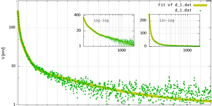
The nature of the transient curve reflects on the charge carrier electrical properties. The transient is composed of different decay components that can be associated with different time constants.
These are called the charge carrier lifetimes, which are widely used quality parameters in the semiconductor and TFT industry. In µ-PCR, the response amplitude is also measured. These values can be used to optimize the TFT fabrication process to get the optimal device performance.
FEATURES
- Optimized for flat panel application
- Stabilized laser source. A feedback control unit is used to give long-term stability to the laser and reduce short-term pulse noise.
- IQ-detection of response. Complex-amplitude transient detection reduces phase-noise of the measurement.
- Adjustable transient analysis method in order to detect advanced electrical properties of the sample
Product Line
FPT
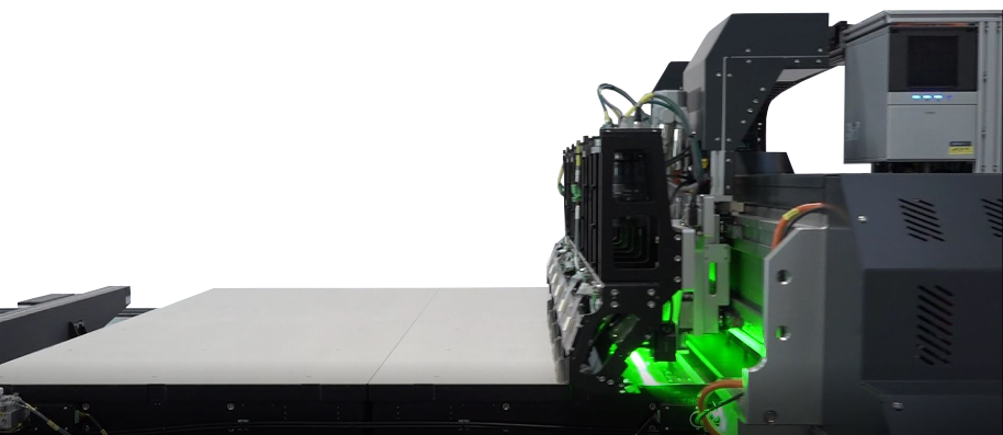
FPT- series are dedicated for flat panel testing and characterization. The products are designed to characterize LCD and AMOLED TFT panels up to GEN 8.5. It is capable to combine several measurement probes into one platform, providing high precision measurements over the entire surface of flat panels with high accuracy and fast motorization stage and weight capacity.
Products

FPT
FPT can be equipped with:
- Spectroscopic ellipsometry
- Spectroscopic reflectometry
- Imaging Spectroscopic reflectometry
- Line mura detection - Chip quality
- Microwave Photoconductive Response - Chip Quality
- Four point probe & six point probe
- Contact angle measurement
- Raman crystallinity
Optical thickness and refractive index of multilayered oxide and semiconductor structures can be determined by spectroscopic ellipsometery at different process steps. The quality of the ELA process can also be monitored by measuring crystallinity, u-PCR and line mura density. Contact angle, stress and resistivity measurements are also available.
The hardware and software are fully controlled by SEMILAB from the design to the integrated software communication with the fab.