Application
METALLIZATION CONTROL
Semilab announced that it had licensed key patents and transferred technology and know-how related to implant monitoring and metal layer characterization from Applied Materials, Inc. The acquired IP covers systems which are capable of junction depth and implant dose measurements, and determination of metal thickness, via and interconnect resistance on product wafers.
Technology
NON-CONTACT SHEET RESISTANCE BY EDDY CURRENT
Device makers have a critical need to measure sheet resistance. Knowing it as a function of position (mapping) allows for optimization of epi reactors to maximize yield.
The Semilab LEI-1510 family allows for non-destructive measurement of sheet resistance. These instruments are optimized for compound semiconductor applications with ranges of operation that dovetail nicely with customer applications. The LEI technology became the process of record in the RF device area with many people asking to see the “LEI” map.
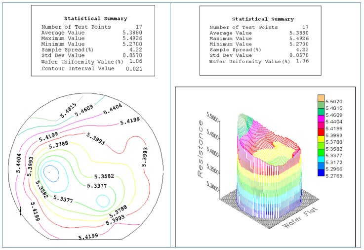 Figure 1. The “Semilab LEI” Maps - the process of record for sheet resitance
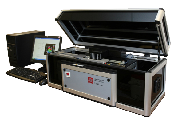
The 1510 Non-destructive Sheet Resistance Measurement System uses eddy current to measure sheet resistance.
Resistivity measurement
Theory of resistivity measurement is based on alternating current in a coil (or pair of coils) inducing alternating Eddy current in a conducting material. The Eddy current measurement is actually the measurement of the electrical loss in the material.
The measured signal depends on:
- Resistivity and thickness, in case of samples with finite thickness as wafers
- Sheet resistance, in case of thin layers
- Distance between the coil(s) and sample
The Eddy current is higher in good conducting material compared to less conductive ones.
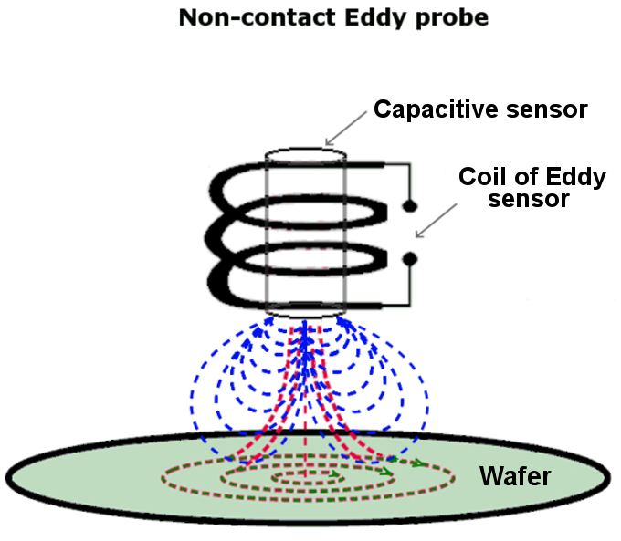
Figure 2. Diagram of Eddy current - upper coil shown only
FEATURES
- Non-destructive
- Non-contact
- No wearing parts unlike 4PP
- Industry standard for RF devices
Product Line
LEI
- Eddy current allows for non-contact sheet resistance
- Ideal for RF device characterization
- Excellent for LED optimization
- Good for metal films on compound characterization