


Application
ION IMPLANT MONITORING
Modern semiconductor devices require precisely controlled dopant concentration and position, and this can be achieved by ion implanting with careful annealing. Typically an n-type species is implanted into a p-type material, or the other way around. Typical species to implant can be boron and indium for the p-type, phosphorus, arsenic and antimony for the n-type layer. Implants are monitored by adding a monitor wafer, and the monitor wafers are checked after the implantation and annealing. Alternatively, the monitoring can be performed by using test boxes on product wafers.
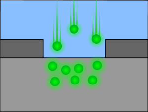 Figure 1. Implantation
Technology
SHEET RESISTANCE MEASUREMENT
The combination of the ion implant process and the process to anneal implants is usually monitored by measuring the sheet resistance of the implanted layer. The sheet resistance varies with dose, energy, and the amount of implanted species that has become electrically active. It is the sheet resistance that ultimately determines the device performance. Thus, measuring sheet resistance is an excellent way to monitor everything associated with an implant process.
The basic idea of the JPV method is the light excitation of the np or pn layer structure, and the pick-up of the resulting junction photovoltage by a capacitive probe. The detected potential is determined by the sheet resistance of the implanted layer, capacitance of junction and resistance through over the diode.
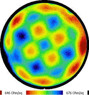
Figure 2. Sheet resistance measurement (lower range)
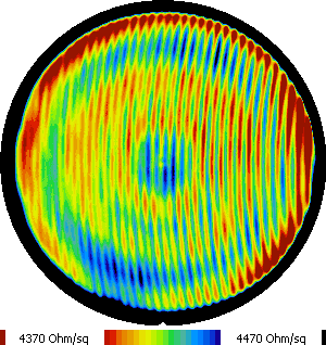
Figure 3. Sheet resistance measurement (higher range)
Semilab offers JPV technology to make non-contact, high resolution fast maps of sheet resistance.
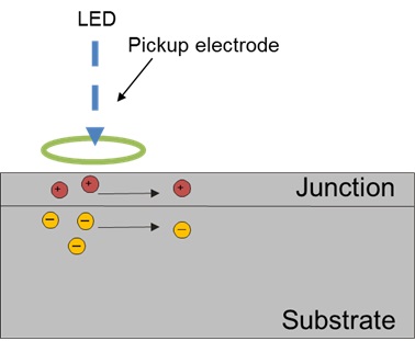
Figure 4. Measurement theory
MEASUREMENT THEORY:
The sample is illuminated by chopped LED light, which generates electrons and holes in the substrate layer. The generated charge carriers diffuse to the junction and the electric field located in the junction separates them. The result of the separation is the change in the junction voltage. This voltage change spread laterally in the implanted layer and the attenuation depends on the sheet resistance, junction capacitance, resistance of the junction and chopping frequency of the LED.
The potential change is detected by a capacitive sensor in order to evaluate the JPV signal, as a function of the frequency of the emitted light.
Based on the evaluation, the sheet resistance (Rs), capacitance of junction (Cd) and the resistance of the diode (Rd) can be calculated.
The junction leakage current is directly connected to the Rd by the following equation:
I_L=kt/q/R_d
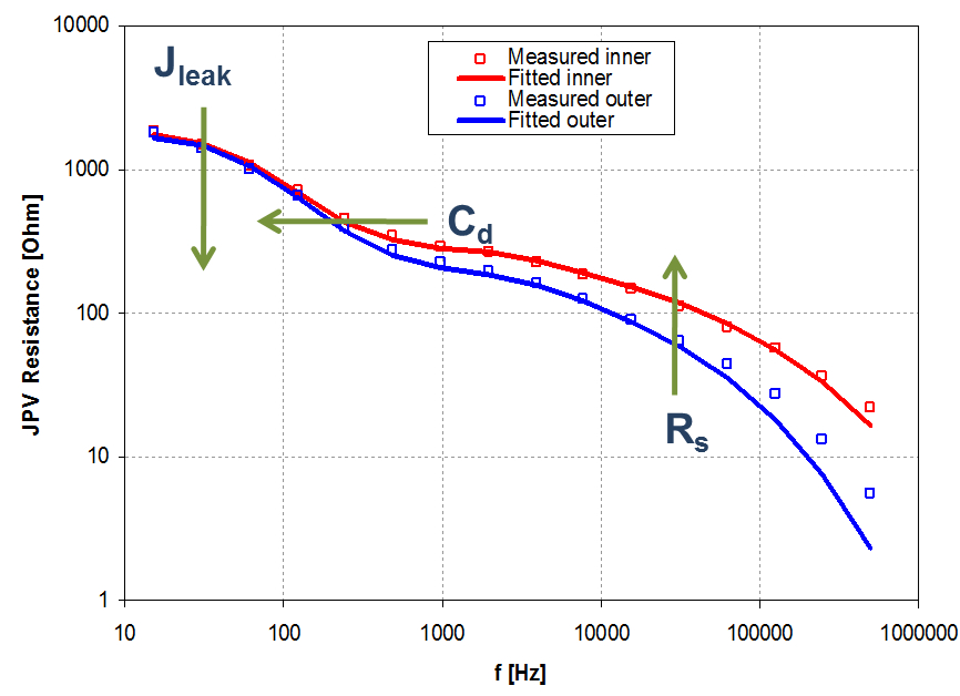
Figure 5. The detected potential is determined by Rs, Cd, Rd and frequency
FEATURES
- Non-contact, non-destructive
- No probe conditioning
- No sample preparation needed
- Works through oxide or coating
- High resolution mapping capability
- Fast mapping
- Good repeatability
Product Line
RT
4 Point Probe (multiple heads) & Non-contact probes (JPV & EDDY) combined in one platform for better operability and long-term stability for wafer makers, device manufacturers and implanter suppliers.
Products

WT-2000 Wafer Tester - Tabletop System
The WT-2000 is a powerful tabletop measurement platform for performing many different semiconductor material characterization measurements. The base system includes all the overhead functions necessary to perform characterization measurements, including power supplies, computer and operating software, X-Y measurement stage and so on. It is typically used to make maps, where the wafer is scanned at a programmable raster. The WT-2000 can also perform measurements at specific, programmable measurement locations.
The WT-2000 is suggested for mid-range fabs and laboratories.
Features and System specifications:
- Wafer size: up to 300 mm with bare or dielectric coated surface
- Wafer handling: manual or Semilab-made indexer
- Loading options:
- 100-200 mm cassette indexer
- 300 mm 13 slot cassette indexer, including open cassettes for 100-300 mm wafers
- 300 mm 25 slot cassette indexer, including FOUP, FOSB, and open cassettes for 100-300 mm wafers
- Samples: np junction (implanted, annealed)
- Automation software with SECS/GEM communication option for non 300 mm standards.
- Factory automation: SECS/GEM for not 300 mm standards
Each system can be configured based on the user’s requirements by adding measurement capabilities and automation capabilities described below.
Measurement capabilities:
Request Info


RT-2201, RT-2500, RT-3000 Sheet Resistance Metrology Systems
Semilab’s new generation sheet resistance measurement systems combine four-point probe (4PP) with non-contact measurement techniques in a variety of platforms from the cost-effective, low automation platform (WT) to full SEMI standard compliant platforms (RT). In addition to the more conventional 4PP, non-contact measurement can be applied to BEOL (metal layers thickness) using EDDY or to FEOL (implant monitoring) using JPV.
Features and System specifications:
- Wafer handling: Robot up to 300 mm
- Inspected area: Full sheet wafers
- Probes: 4PP (FEOL & BEOL) , EDDY (BEOL) , JPV (FEOL)
- 1-4 permanent 4PP heads for different ranges & applications, Lower CoO
- Cleanroom class: class 1 minienvironment
| Specification | RT-2201 | RT-2500 | RT-3000 |
|---|---|---|---|
| Wafer Size | up to 200 mm | 150/200 mm or 200/300 mm | 200/300 mm |
| Loading options | 2 open cassettes up to 200 mm |
|
Double FOUP platform |
| Automation software | SECS/GEM communication option | SECS/GEM communication option | Fully automated software |
| Factory automation |
Not available |
Not available, designed for mid-range fabs | Yes, specifically designed for high volume facilities with full factory automation, OHT option |
It is possible to integrate all of the following measurement techniques into one mapping instrument:
- Eddy current technique for thin layers' sheet resistance measurements
- Junction Photovoltage measurement for sheet resistance mapping
- Ion Implant Monitoring
RT product line is designed to meet SEMI standards.
Request Info