


Application
EPI RESISTIVITY MEASUREMENT
A blanket layer of silicon can be added to a silicon substrate by a CVD process to achieve changes in the properties, like resistivity, type and defect density. This CVD process is called epi (or epitaxial) deposition. The thickness monitoring of the epi layer is part of the production process of making the epi wafers. This monitoring is executed on a sample basis, or only to confirm that the epi reactor is set up properly.
Semilab can offer non-contact optical solution for Epi thickness monitoring, depending on infrared reflection techniques.
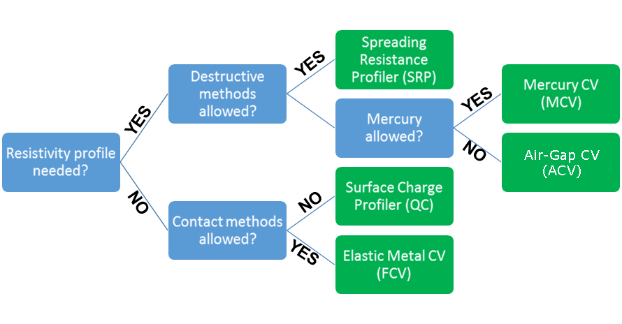 Figure 1. Resistivity measurement flow
Technology
SURFACE CHARGE PROFILING
Alternating current SPV analysis (ac-SPV)
The ac-SPV is an electro-optical method, which allows rapid and non-destructive characterization of the electric properties of a bare semiconductor surface, or one covered with an insulator of several microns thickness. The method provides simultaneous determination of critical parameters, such as the near-surface doping concentration, resistivity, surface lifetime and surface conductivity type.
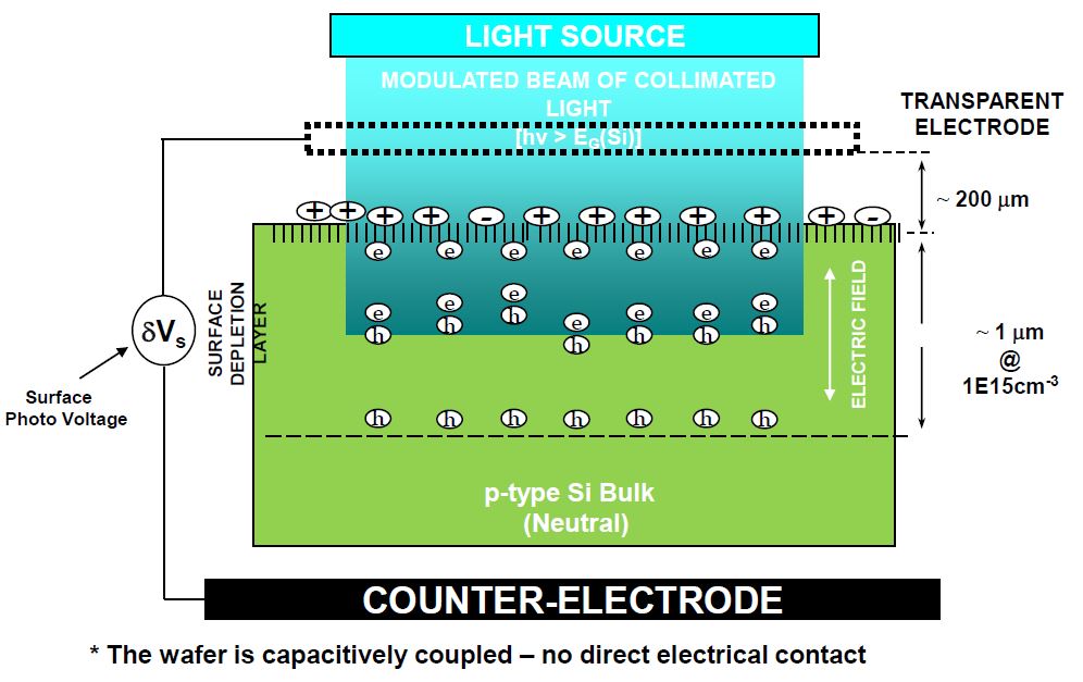
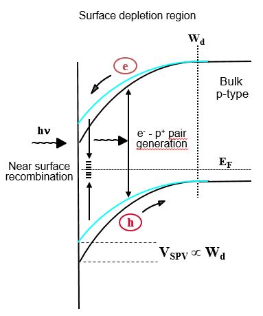 Figure 2. ac-SPV analysis
PRINCIPLES OF OPERATION
The ac-SPV method based on measurements of the change of the initial surface barrier height, due to chopped (sinusoidal) light illumination incident on the wafer surface (ac-Surface Photovoltage measurement). The surface potential barrier is formed at the surface due to presence of interface (surface) state charge and charge in the dielectric film (oxide charge) on the wafer. The used photon energy is greater than the semiconductor bandgap and the semiconductor surface is kept in depletion or inversion with a superimposed electric filed. The induced ac-SPV signal can be detected via capacitively-coupled electrode and is proportional to the depletion layer width. It can be used to calculate other important electrical parameters of the surface region determined by the depletion layer width.
In order to achive stable inversion is necessary to apply pre-treatment – grow an oxide on the wafer’s surface in the UV Chambers and apply Corona charge.
For n-type wafer negative, for p-type wafer positive corona charge is applied in steps until the inversion is reached automatically. It is necessary that the applied corona charge remains stable on the surface during the measurement to maintain the inversion condition. This condition is satisfied when there is a thin good quality oxide presents on the wafer surface.
In case of UV chamber the wafer is illuminated in stagnant CDA environment which ensures uniform and dense ozone layer above the wafer i.e. fast and uniform oxidation.
Desorber is used to clean organic contamination from the wafer and to eliminate hydrogen boron pairs.
FEATURES
- Non-destructive, non-contact
- High resolution mapping capability with rapid speed
- Capable of measuring thin EPI and Epi over buried layers
- Earliest detection of EPI reactor problems
- Eliminates resistivity monitor wafers
- Low cost of ownership
- Robust performance/easy operation
- Standard for wafer manufacturers
Product Line
QC
The QC series uses non-contact ac-Surface Photo Voltage technology to perform non-destructive measurements of near-surface resistivity, doping concentration and recombination lifetime on as-grown epitaxial wafers.
For more than 10 years QC Solution instruments have been used for epi and annealed Chochralsky process control by many wafer and IC manufacturers.
Products

QC-series
Semilab’s QC platforms (Near Surface Doping Mappers) for epitaxial monitoring are the only non-contact, non-destructive, high throughput systems that can reliably map near surface doping on process wafers.
Features:
- Integrated universal (for both p- and n-type) UV/Corona pre-treatment with improved and optimized UV oxidation for up-to 300 mm wafers and accurate feedback loop controlled corona charging technique with new mechanical and electronics design and new corona system.
- New sensor design insensitive to wafer/chuck flatness.
- Rapidity of even full wafer mapping measurements ensures an impressive throughput and the ability to monitor and control the epitaxial process
- Improved new software has multiple benefits, such as: highly configurable, multitasking, real-time data monitoring, simplified recipe generation, job queuing and fully 300mm SECS/GEM complaint.
- Wafer motion stage with precise positioning
- Detects problems that may escape other metrology techniques, because of the strong surface sensitivity
- Qualifies Epi layer within the critical device region of IC
- Provides near-surface carrier lifetime as an indicator of wafer contamination
- Fast full wafer mapping capability
- Measures all doping combinations: n/p, n/n, p/n, p/p
| QC-2200e | QC-2500e | QC-3000e | |
|---|---|---|---|
| Wafer size | up to 200 mm |
up to 300 mm |
up to 300 mm |
| Platform | Full hand-off automated | Full hand-off automated | Full hand-off automated |
| Load port | 1 loadport / FOUP | 1 loadport / FOUP | 2 loadports / FOUP |
|
Primary applications:
|
|
|
| Equipments: | Measurement parameters: | Measurable wafer types: |
|
|
|
Request Info