


Application
THIN FILM APPLICATIONS
In order to keep the thin film solar cell production stable, the adequate control of the layer deposition and treatment processes is crucial. Semilab offers several metrology solutions for the characterization of electrical and optical properties of the thin layers.
Our special design Four-Point-Probe and Eddy Current sensors provide accurate measurement of the sheet resistance of thin semiconductor, TCO or even metal layers in the total range of interest.
Using Semilab’s Spectroscopic Ellipsometry and Spectroscopic Haze and Reflectance techniques the complete characterization of the layer thickness and other optical parameters can be accomplished even on multilayer structures.
.png)
Technology
VISUAL INSPECTION
Visual inspection technology combines two key technologies and tools, the Spectroscopic Ellipsometer and IN-CORE Systèmes’ high-resolution image processing systems, 2D-3D line-scan camera based for defect detection and dimensional measurements of various surface characteristics. The platform was developed specifically for printed PV (organic and perovskite) applications.
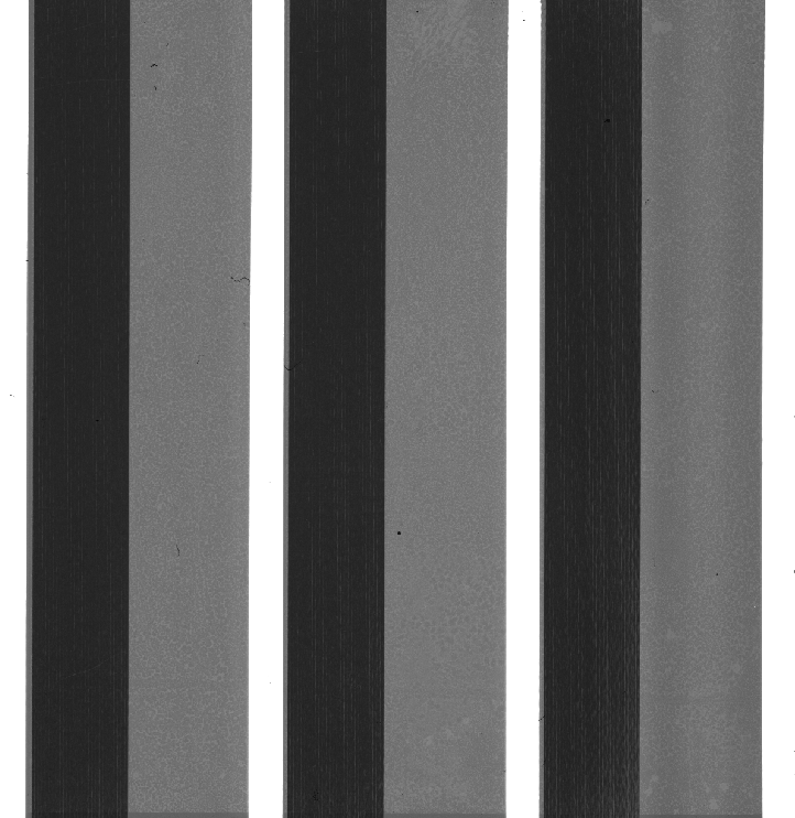 Example of Linear Vision
The tool is designed to inspect and measure at highest precision on large area, 300 x 300 millimeter, flexible plastic or glass substrates, the new platform provides non-contact, fully automated defect detection and location. Furthermore the system provides advanced metrology capability which has been optimized for the OPV complex process, and is capable of analyzing single and multilayer structures.
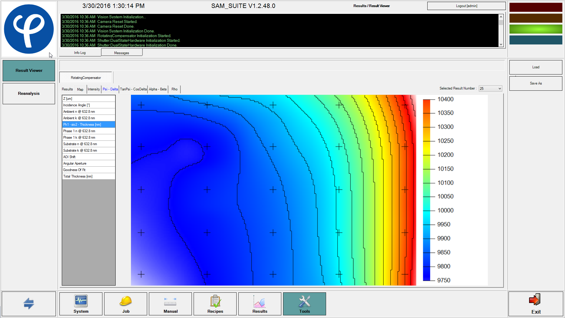
Result evaluation is realized with help of Semilab software.
FEATURES
- Non-contact, non-destructive measurement method
- Accurate determination of the quality of the printed materials and structures
- Analyzing of single and multilayer structures
- Larger size substrates
- Roll-to-roll in-line control possibility
Product Line
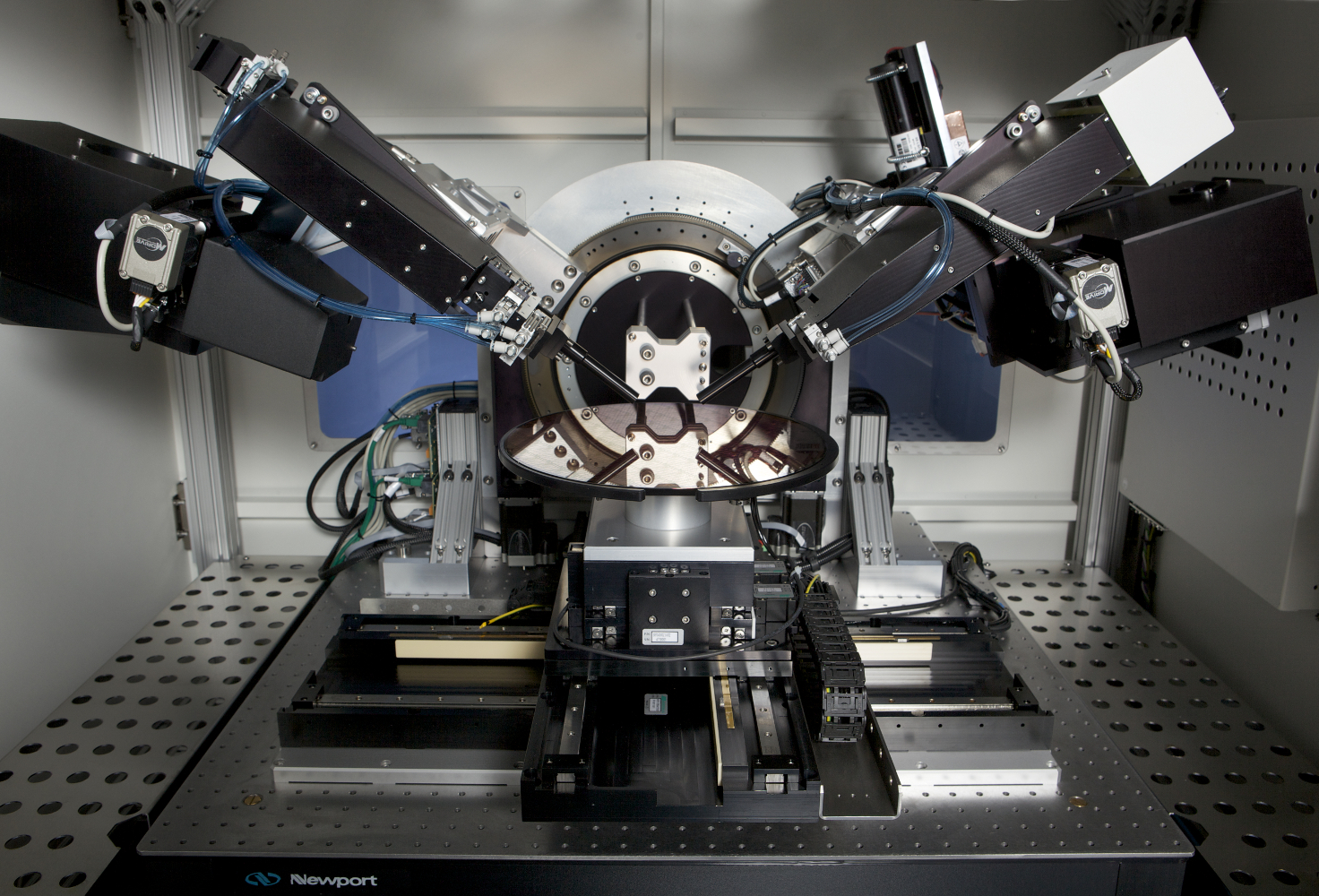
SE
The SE series have a unique Modular Optical Platform including a spectroscopic ellipsometer with rotating compensator optics. The system has strong modular and versatile design, to answer needs from simple single layer thickness to more demanding applications such as those combining polarimetry, scatterometry and ellipsometry using Mueller matrix. It has a unique independent arm angle selection, and small spot size.
Products

SE-2100
Printed Electronics. Optical & Electrical Metrology. Thin Film Coating characterization. Layer Thickness control.
Features and System specification:
- Capable for Fast and accurate measurement on square samples up to 350x450 mm or wafers up to 300 mm
- Special design of the chuck to hold Flexible Sample
- Active Vibration damping
- High-resolution mapping stage
- Fast Omron autofocus
- Vertical camera for samples visualisation & Pattern recognition
- Joystick to move the sample easily
- CE and SEMI standards compliant
Components & Options:
- Spectroscopic Ellipsometer:
- Fast acquisition directly on the foil
- Measurement Spot adapted for Plastic substrate
- Spectroscopic Reflectometer:
- For reflection and transmission of the films
- Non-contact Sheet resistance:
- Fast and accurate Sheet resistance by Eddy Current
- For Transparent electrode and Metal
- Other measurement technique like Raman, Lifetime...etc
Applications:
- Display: TFT, OLED on Glass or Flexible substrate
- Lighting: New OLED Lighting application. White OLED
- Printed Electronics: Any process on flexible substrate (transistor, sensors, etc.)
- Photovoltaics: Small Thin Films PV panels, TCO panels