Application

CHARACTERIZATION OF 3D STRUCTURES


Driven by the continued demand for increased functionality in integrated circuits, the trend toward ever-higher levels of integration has resulted the use of increasingly three-dimensional structures in order to gain more functions out of a given area. This is evident in several areas of both device and interconnect technology. One example is the continuing trend toward higher aspect ratios in vias, contacts and memory capacitor structures. Another example is the adoption of vertically-oriented transistor channels within FinFET logic devices at advanced technology nodes. On a much larger length scale, the use of through-silicon via (TSV) structures to create 3D interconnects enables vertical stacking of multiple dies. Each of these three developments leads to new challenges in process control and metrology, and a common theme is required between them to measure profiles and depths of etched structures. While diagnostic techniques, such as SEM, AFM and SPM play an important role in characterizing processes, optical metrology methods are highly desired, because they provide rapid measurements on product wafers, enabling routine monitoring and advanced process control.

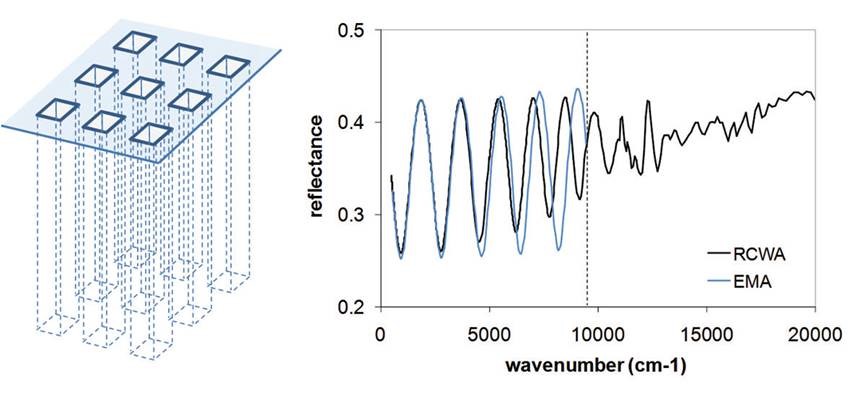
Figure 1. 3D array of square trenches in silicon (left) and corresponding simulated infrared spectra (right), illustrating agreement between RCWA and EMA calculation methods in the long wavelength limit.


Model-based infrared reflectometry (MBIR) combines a photometrically accurate FTIR measurement system with a spectral range of 1-20 μm, and model-based analysis of reflectance spectra from multilayered films and structures. The infrared wavelength range provides unique advantages for the measurement of 3D-etched structures, which have already been exploited in applications of MBIR for various structures, including memory capacitors, power device trenches and isolation trenches.

One principle advantage of the infrared metrology is the simplified modeling of complex periodic structures. At wavelengths, greater than the pitch of a structure, the light propagates through the structure as if it was a homogeneous medium with an effective refractive index. This can be calculated from the geometry of the structure and the refractive indices of its component materials by using an effective medium approximation (EMA). If the structure parameters, such as trench width vary with depth, it is modeled as a stack of multiple layers, each characterized by its own effective refractive index. Therefore the problem of modeling the optical response of a complex etched structure can be reduced to the simpler problem of modeling a multilayer stack.

To illustrate this point, see the example presented in Figure 1. The figure shows simulated spectra for 45 degrees incidence and S-polarization for an array of square trenches etched in silicon. The trenches are 1 micron deep, have a pitch of 0.25 microns and have a width of 0.125 microns. The figure shows both an exact calculation using rigorous coupled-wave analysis (RCWA) and a simplified calculation using a Maxwell-Garnett type EMA. A vertical line corresponding to about 10,000 cm-1 (that is a wavelength of 1 micron) indicates the “diffraction threshold”, WHERE the first transmitted diffraction order emerges. In the short-wavelength range to the right of the threshold there is a rather complex spectrum typical for scatterometry. In the infrared range to the left of the threshold, the diffraction is absent. The spectrum comprises a regular pattern of interference fringes arising from the interference of light reflected from the top and bottom of the trench structure. As per the figure, the fringes can be well approximated by using the EMA method. Parameters of the structure, such as trench depth and width are readily determined from the period and amplitude of the fringes. Thus the long-wavelength approach greatly simplifies the measuring of 3D-etched structures. Note that the advantage is not only in the ease of modeling, but also in the fact that infrared spectra themselves are rather simple and their relationship to the parameters of the structure can be readily understood.

Technology