Application
CONTAMINATION MONITORING
Semilab’s suite of non-contact metrologies lead the IC industry for in-line detection of ultra-low metallic contamination. Semilab offers full wafer imaging solutions, ranging from the high throughput Photoluminescence Imaging technique (PLI) to more well-established lifetime-based methods, including Suface PhotoVoltage (SPV) and microwave Photoconductance Decay (µ-PCD). The flagship digital SPV technology (FAaST system) is industry standard that leads the world in bulk Fe detection.
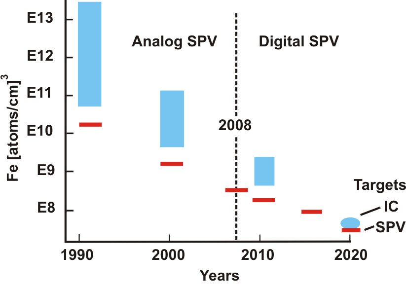
There is no disputing the detrimental effect of metallic contamination on the integrity of the critical gate oxide used in integrated circuits. During high temperature processing, contamination in the silicon wafer often precipitates as a defect at the Si/Dielectric interface or segregates to the dielectric – in either case it has the potential to cause premature device failure and a reduction in product yield. The probability of metallic contamination impacting yield is a function of the chip size (e.g. technology node/critical dimension) and the defect density (e.g. the amount of contamination), such that as device dimension decrease, maintaining yield requires a corresponding reduction in contamination. Figure 1 clearly demonstrates the reality of this relationship over the past 25 years, during which time the IC industry has experienced a more than 3 orders of magnitude reduction in typical background Fe concentration observed in new fabs. More importantly the near term projection, where another order of magnitude reduction is needed to meet the requirements of the state-of-the-art Si IC manufacturing, with white pixel reduction in CMOS image sensors being a major stimulus for this effort.

Figure 1. Typical background Fe concentration in new IC Fablines (blue) and the state-of-the-art SPV detection limit (red)


