


Application
CONTAMINATION MONITORING
Semilab’s suite of non-contact metrologies lead the IC industry for in-line detection of ultra-low metallic contamination. Semilab offers full wafer imaging solutions, ranging from the high throughput Photoluminescence Imaging technique (PLI) to more well-established lifetime-based methods, including Suface PhotoVoltage (SPV) and microwave Photoconductance Decay (µ-PCD). The flagship digital SPV technology (FAaST system) is industry standard that leads the world in bulk Fe detection.
There is no disputing the detrimental effect of metallic contamination on the integrity of the critical gate oxide used in integrated circuits. During high temperature processing, contamination in the silicon wafer often precipitates as a defect at the Si/Dielectric interface or segregates to the dielectric – in either case it has the potential to cause premature device failure and a reduction in product yield. The probability of metallic contamination impacting yield is a function of the chip size (e.g. technology node/critical dimension) and the defect density (e.g. the amount of contamination), such that as device dimension decrease, maintaining yield requires a corresponding reduction in contamination. Figure 1 clearly demonstrates the reality of this relationship over the past 25 years, during which time the IC industry has experienced a more than 3 orders of magnitude reduction in typical background Fe concentration observed in new fabs. More importantly the near term projection, where another order of magnitude reduction is needed to meet the requirements of the state-of-the-art Si IC manufacturing, with white pixel reduction in CMOS image sensors being a major stimulus for this effort.
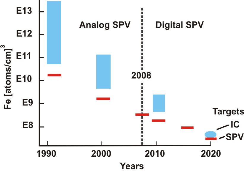
Figure 1. Typical background Fe concentration in new IC Fablines (blue) and the state-of-the-art SPV detection limit (red)
Technology
MINORITY CARRIER LIFETIME MEASUREMENT
Lifetime is a property of the bulk semiconductor material. It is the average amount of time an excess carrier exists in a semiconductor material before recombining to achieve equilibrium. The same parameter is also called “minority carrier lifetime”, “carrier lifetime” and “recombination lifetime.” The lifetime of a semiconductor is long with a perfect crystal lattice and no comtamination. Any imperfections in the semiconductor material or contamination reduce the lifetime. Thus, monitoring lifetime is an excellent method to detect contamination.
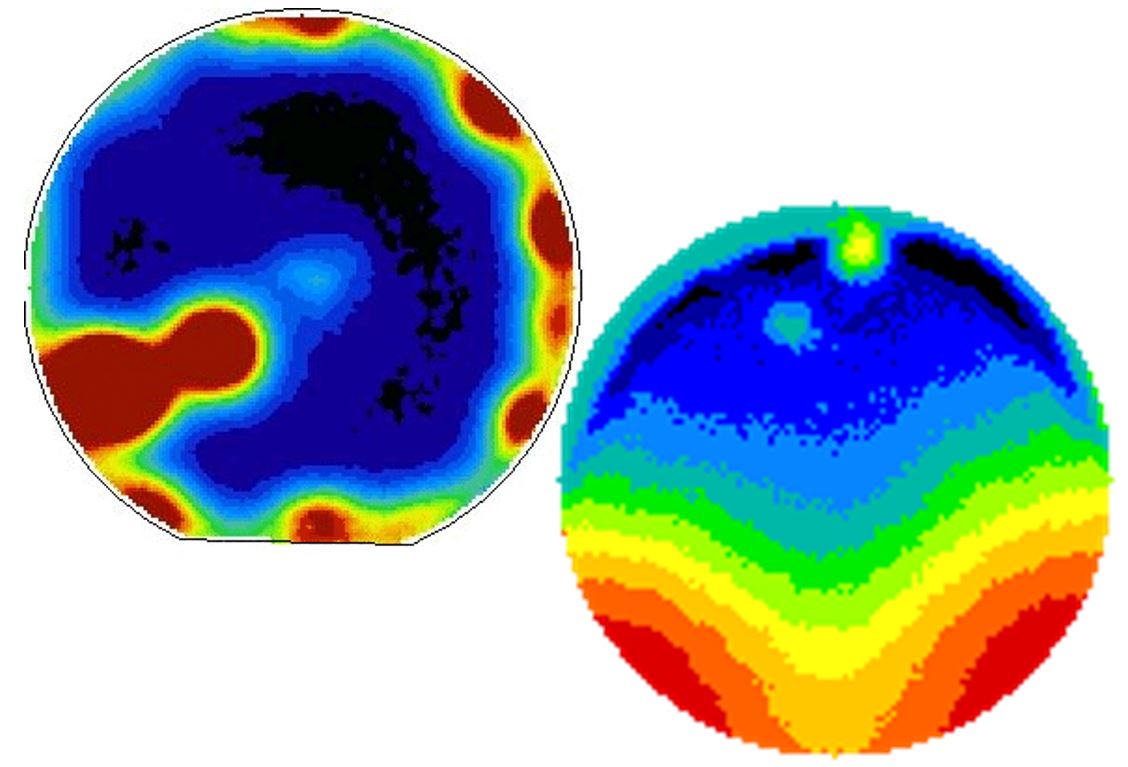 Figure 4. Measurement maps
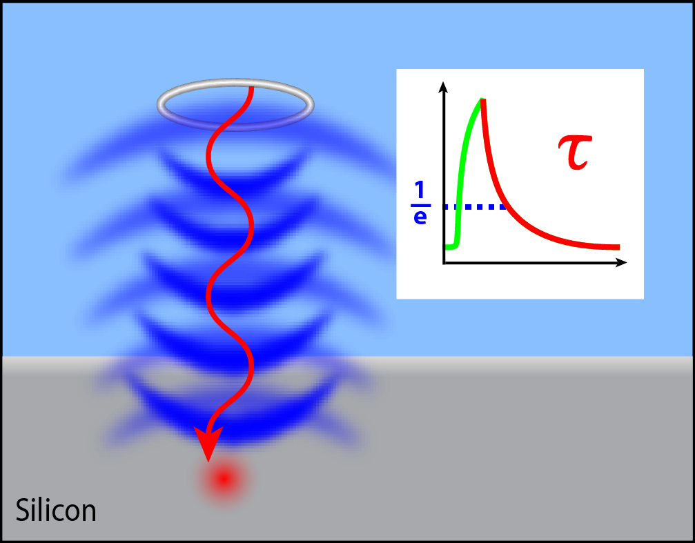 Figure 5. Measurement theory
The most common way of measuring lifetime is with the so-called microwave PCD (µ-PCD) technique.
µ-PCD is based on the excess carrier generation by laser pulse, which effects the change in conductivity and thus microwave reflectivity. After the illumination the conductivity decays by recombination, which can be monitored by measuring microwave reflectivity as a function of time. Lifetime is determined from the recorded decay transient. To achieve the best result, the surface recombination needs to be eliminated by passivation. Semilab offers a special treatment chamber to achieve an optimum surface without the usage of wet chemicals.
Crystal Growth Defects:
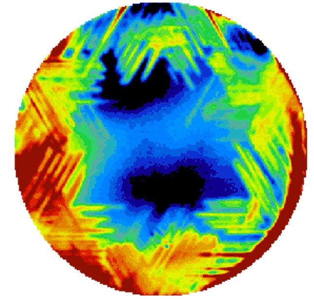
Figure 6. Slip lines
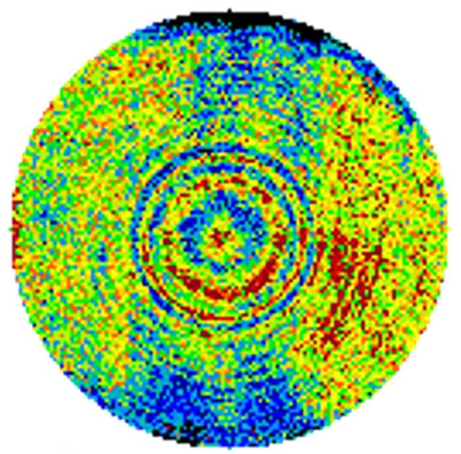
Figure 7. Oxygen striations
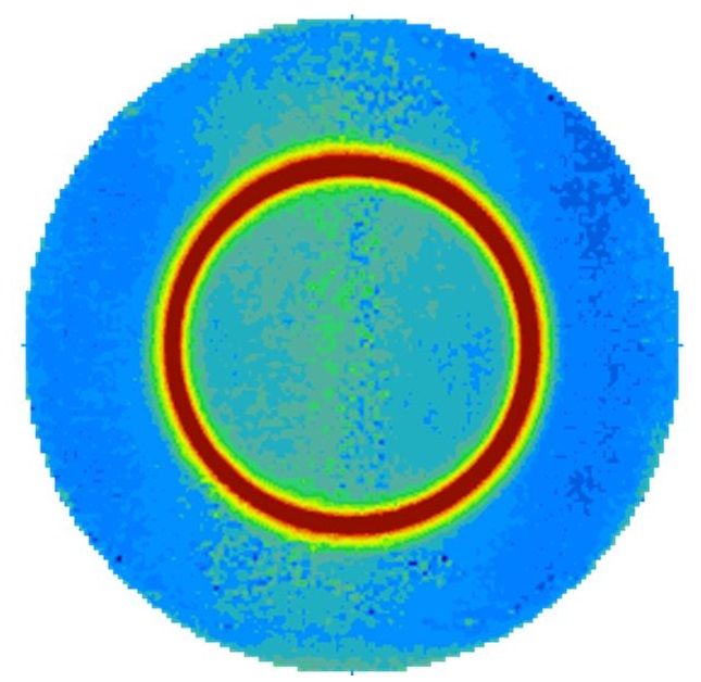
Figure 8. OSF ring
Process induced defets/Fe mapping:
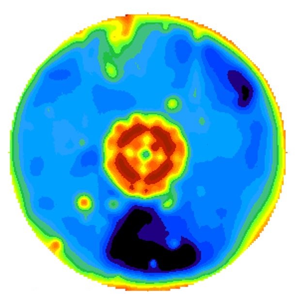
Figure 9. Contaminated vacuum chuck
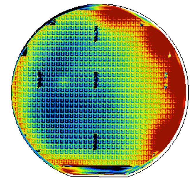
Figure 10. Boat contamination
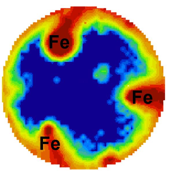
Figure 11. Fe detection
FEATURES
- Detects:
- impurities due to heavy metal contamination and transition metal contamination
- crystal defects
- iron concentration determination both in CZ and FZ wafers
- No wafer thickness limitation
- High lateral resolution
- Requires surface passivation: thermal oxide, chemical passivation or corona charging
Product Line
WT
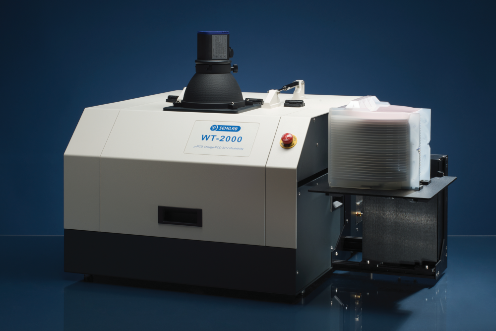
The WT product line is a powerful measurement platform for performing many different semiconductor material characterization measurements. The base system includes all the overhead functions necessary to perform characterization measurements, including power supplies, computer and operating software, X-Y measurement stage and so on. The WT-2000 is typically used to make maps, where the wafer is scanned at a programmable raster. Each system is configured to the user’s requirements by adding treatment and measurement capabilities.
Products

WT-2000MCT
Temperature Dependent Lifetime Measurements for Characterization of Narrow-Band Semiconductors
The WT-2000MCT is a special design for µ-PCD lifetime measurement at different sample temperatures.
Features and System Specifications:
- Sample size: maximum 100 mm in diameter
- Temperature range: from 80 K to 325 K
- Cooling time: < 0.2 K
Operating modes:
- Whole wafer mapping at a preselected stabilized temperature
- Single-point lifetime scan as a function of temperature
Applications:
- Minority carrier lifetime as a function of temperature
- Excels in measuring lifetime in narrow band semiconductors, where excess carriers are thermally excited at room temperature
- Materials: HgCdTe, InSb, GaAs, etc.
Request Info

WT-2000
The WT-2000 is a tabletop tool, suggested for mid-range fabs and laboratories.
Features and System Specifications:
- Wafer size: up to 300 mm with bare or dielectric coated surface
- Wafer handling: manual or Semilab-made indexer
- Loading options:
- 100-200 mm cassette indexer
- 300 mm 13 slot cassette indexer, including open cassettes for 100-300 mm wafers
- 300 mm 25 slot cassette indexer, including FOUP, FOSB, and open cassettes for 100-300 mm wafers
- Objectives of detection:
- Impurities due to heavy metal and transition metal contamination
- Crystal defects
- Optional iron concentration determination both in CZ and FZ wafers
- No wafer thickness limitation
- Fast measurement speed
- High lateral resolution
- Required surface passivation: thermal oxide, chemical passivation or corona charging
Each system can be configured based on the user’s requirements by adding measurement capabilities and automation capabilities described below.
Measurement capabilities:
- µ-PCD for measuring carrier lifetime
- SPV for measuring diffusion length
- JPV for measuring ion implants
- Eddy current measurement of sheet resistance
Request Info

WT-2200, WT-2500, WT-3000
WT series are powerful stand-alone tools specifically designed for high volume 300 mm facilities with full factory automation and OHT included.
Features and System Specifications:
- Wafer handling: Robot up to 300 mm
- Cleanroom class: class 1 minienvironment
- Treatments:
- Hot chuck / desorber
- Linear corona charger and pin charger
- Optical flash
- High temperature RTP
| Specification | WT-2200 | WT-2500 | WT-3000 |
|---|---|---|---|
| Wafer Size | up to 200 mm | 150/200 mm or 200/300 mm | 200/300 mm |
| Loading options | up to 4 pieces of 200 mm open cassette |
|
Double FOUP platform |
| Automation software |
SECS/GEM communication option |
SECS/GEM communication option | Fully automated software |
| Factory automation | Not available, designed for mid-range fabs | Not available, designed for mid-range fabs | Yes, specifically designed for high volume facilities with full factory automation, OHT option |
It is possible to integrate all of the following measurement techniques into one mapping instrument:
- Microwave induced photoconductive decay
- (µ-PCD) and Charge-PCD / minority carrier lifetime mapping
- Surface Photovoltage (SPV) / diffusion length mapping
- Iron (Fe) concentration mapping
WT product line is designed to meet SEMI standards.
Request Info