


Application
DIELECTRIC POROSITY MEASUREMENT
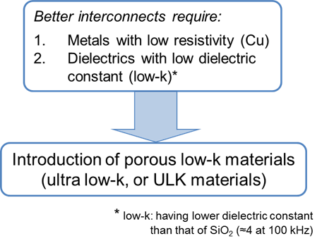
Porous films in microelectronics
- For decreasing the capacitance of interconnection isolators in integrated circuits:
- Decrease of RC time delay (increase of operating frequency)
- Decrease of power consumption
- For further decreasing the dielectric constant, the material has to be porous
- This implies additional reliability questions, eg.:
- Cracking / adsorption loss (need to stay on the substrate for long)
- Mechanical strength (need to survive chemical-mechanical polishing, CMP)
- Typical Young modulus of SiO2 is 70 GPa (for dense SiOCH: <15 GPa, for porous SiOCH: <10 GPa)
- Moisture absorption (need to be hydrophobic, in order to remain a good insulator)
- Dielectric constant depend on porosity, eg. for porous SiOCH*:
- ULK (ultra low-k): k ≈ 2.5 , with porosity ≈ 20% and pore size ≈ 3-4 nm
- ELK (extreme low-k): k ≈ 2.3, with porosity ≈ 30% and pore size ≈ 5-6 nm
- This implies additional reliability questions, eg.:
- Characterization of porous dielectric layers is necessary to ensure reliable layer fabrication
Technology
ELLIPSOMETRIC POROSIMETRY
Ellipsometry Porosimetry (EP) measures the change of the optical properties and thickness of the materials during adsorption and desorption of a volatile specie either at atmospheric pressure (EPA) or under reduced pressure depending on the application (EP). The EP technic is unique by its ability to measure porosity of very thin films down to 10nm, reproducibility and its speeds of measurement. Compares to traditional Porosimeter, Ellipsometer porosimeters is well suited for very thin film pore size and pore size distribution measurement. Film porosity is a key factor in Silicon based technology using low k materials, organic industry (encapsulated OLED\'s) as well as in the coating industry using SolGel technics.
Ellipsometry porosimetry (EP) technology was patented by IMEC and licensed exclusively to Semilab.

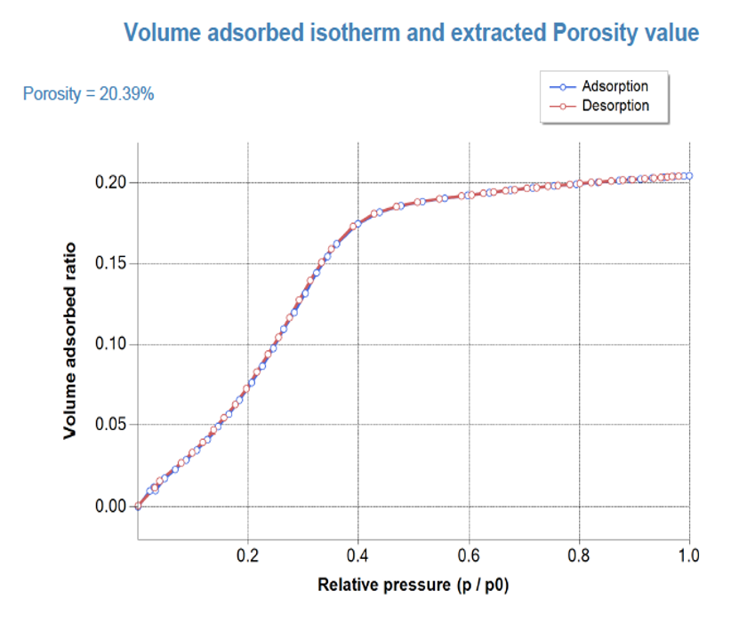
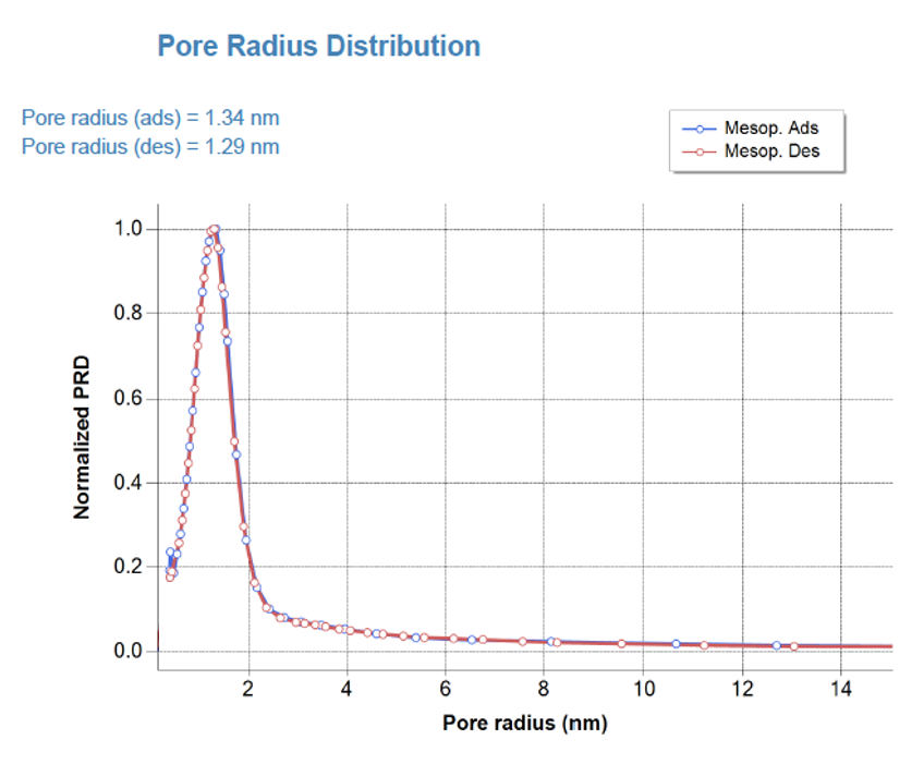
Ellipsometric Porosimetry (EP) measures the changes in optical properties and thickness of porous thin films by spectroscopic ellipsometry (SE) during an adsorption cycle of an organic solvent. These changes occur as the pores in the material are being filled by the adsorptive. From the measured refractive Index and thickness behavior during the adsorption cycle, specific layer properties can be deduced: Porosity, Pore size distribution and characteristic pore size, Young’s Modulus, hydrophobicity (water penetration), diffusion coefficient.
Semilab propose two type of adsorption cycle setup: At atmospheric pressure, (EPA) with water as solvent or under vacuum (EP) with many different organic adsorptive (Toluene, IPA, Methanol, Ethanol, Water, ect.).
The technique can access both micro porosity (Pore diameter < 2nm) and meso porosity (2 > Pore diameter > 50nm) and can be used on layers from 10nm to several µm depending on the instrument configuration. Compared to traditional Porosimeter, EP does not require sample preparation or film scratching and are well suited for very thin film pore size and pore size distribution measurement. It is a unique technique by its ability to measure porosity of both single and multilayers thin film structures, with excellent reproducibility and measurement speed.
APPLICATIONS to EP technique are numerous as thin film porosity is a key factor in Silicon based technology using low k materials or porous Silicon films, Photovoltaic with metal oxides (SiO2, TiO2, W2O3..) for Dye sensitized solar cells, organic electronic with the permeability of the barrier layer for OPV or OLED (encapsulation) as well as in the coating industry using SolGel technique.
FEATURES
EP technique provides reliable and precise measurements of:
- thickness
- refractive index
- porosity
- diffusion coefficient
- pore size distribution and Young modulus of porous thin films such as ultra low K, porous Silicon, nanoparticle layers, metal oxides or barrier layers integrity
- sealing efficiency
Product Line
PS
PS products are well suited to characterize materials for many applications such as:
- Membranes (water permeability for OLED or OPV applications)
- Storage (fuel cells)
- Sensors (biomaterials, nanomedicine…)
- Catalysis surfaces
- Nano-structure and nano-composite materials
- Hybrid organic & inorganic interfaces…
Products

PS-2000, PS-2500
Semilab Porosimeter Series (PS) metrology systems use Ellipsometry Porosimetry (EP) technique to provide reliable and precise measurements of thickness, refractive index, porosity, pore size distribution and Young modulus of porous thin films such as ultra-low K, porous Silicon, nanoparticle layers, metal oxides or barrier layers integrity... Combining solvent adsorption experiments in a high vacuum chamber to Semilab Spectroscopic Ellipsometry (SE) technology, the PS systems form a comprehensive metrology solution, helping our customers to develop, qualify and monitor current and future processes and especially solve the integration challenges of porous low K materials.
The PS Product Family presents various degrees of automation and wafer size capabilities from coupons to 450mm wafers. Its unique technology enables the structural characterization of CVD and spin coated porous thin film without sample scratching or preparation.
An optional heated chamber, available on 300mm selected models, provides advanced measurement capability such as film annealing or Uniaxial Coefficient of Thermal Expansion (CTE), helping chipmakers identify process issues that can lead to film collapse or cracks.
In our fully automated PS-2500 model, a preheating / cooling station allows desorption of residues or organic materials and moisture from the pore before / after measurement, making sure the total accessible porosity is measured and that no solvent remains in the pores if further processing is needed.
Configurations:
| Sample size | Name | Mapping | Features |
|---|---|---|---|
| Up to 300 mm | PS-2000 | Yes | Manual loading automated transfer Optional Heated chamber for CTE measurements |
| 300mm | PS-2500 | Yes |
Fully automated, 1 load port (300 mm) |
Dual load port with OHT available with PS-3000.
Please contact us for 450 mm wafer capable platforms.
PS instruments can also be used to qualify the sealing layer of both patterned and blanket wafers: the instrument detects the diffusion of solvent through the sealing layer, which leads to a change in refractive index measured by Spectroscopic Ellipsometry. Finally, any PS product is also a traditional spectroscopic ellipsometer, which can address characterization needs of non-porous thin films.
Ellipsometry porosimetry (EP) technology was patented by IMEC and licenced exclusively to Semilab.
Request Info