


Application
THIN FILM THICKNESS MEASUREMENT
As the semiconductor industry continues to fulfill Moore’s law, thin film thickness is one of the most rapidly scaled dimensions. Consequently, chip manufacturers must implement metrology systems that will be effective for statistical process control of ultra-thin dielectrics.
Ellipsometry is a non-destructive technique, capable of being used for any transparent and semitransparent medium. It can measure a wide range of layer thickness from a fraction of mono-atomic layer to several micrometers.
Ellipsometry allows the determination of the thickness of single layers and multi-layer stacks. In addition, it allows the absolute characterisation of optical properties of materials by extraction of the N and K data.
Using Spectroscopic Ellipsometry, up to 7 layers can be analysed simultaneously in one measurement in order to extract the thickness of every individual layer. Material optical properties also, can be obtained over a wide spectral range, from Deep UV to near InfraRed.
Unlike other optical techniques, this method requires neither reference sample nor reference beam like reflectometry. Moreover, ellipsometry has the advantage of high sensitivity due to the additional measurement of the phase of light at different wavelengths. As a consequence, it allows analysis of complex structures like multi-layers with rough interfaces and unknown material composition.
Technology
SINGLE-WAVE ELLIPSOMETRY
Laser ellipsometry measures a change in polarization as light reflects or transmits from a material structure. The polarization change is represented as an amplitude ratio, Ψ, and the phase difference, Δ. The measured response depends on optical properties and thickness of individual materials. Thus, ellipsometry is primarily used to determine film thickness and optical constants. However, it is also applied to characterize roughness and surface morphology by using scatter light measurement method.
FEATURES
- Non-destructive
- Non-Contact measurement method
Product Line
LE
Applications: tunnel oxide (thin SiO2 on Si), and poly-Si on SiO2/Si wafer structures monitoring
Products

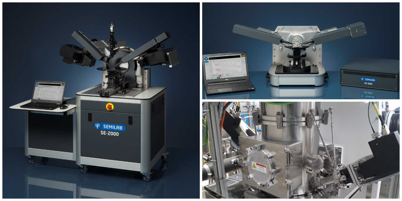
LE-5100
Combined Laser ellipsometer and spectroscopic reflectometer with an X-Y high precision stage. It measures thickness and optical properties (n and k) of mono and multilayer. The measurement is non-destructive and non-contact.
Features and System specifications:
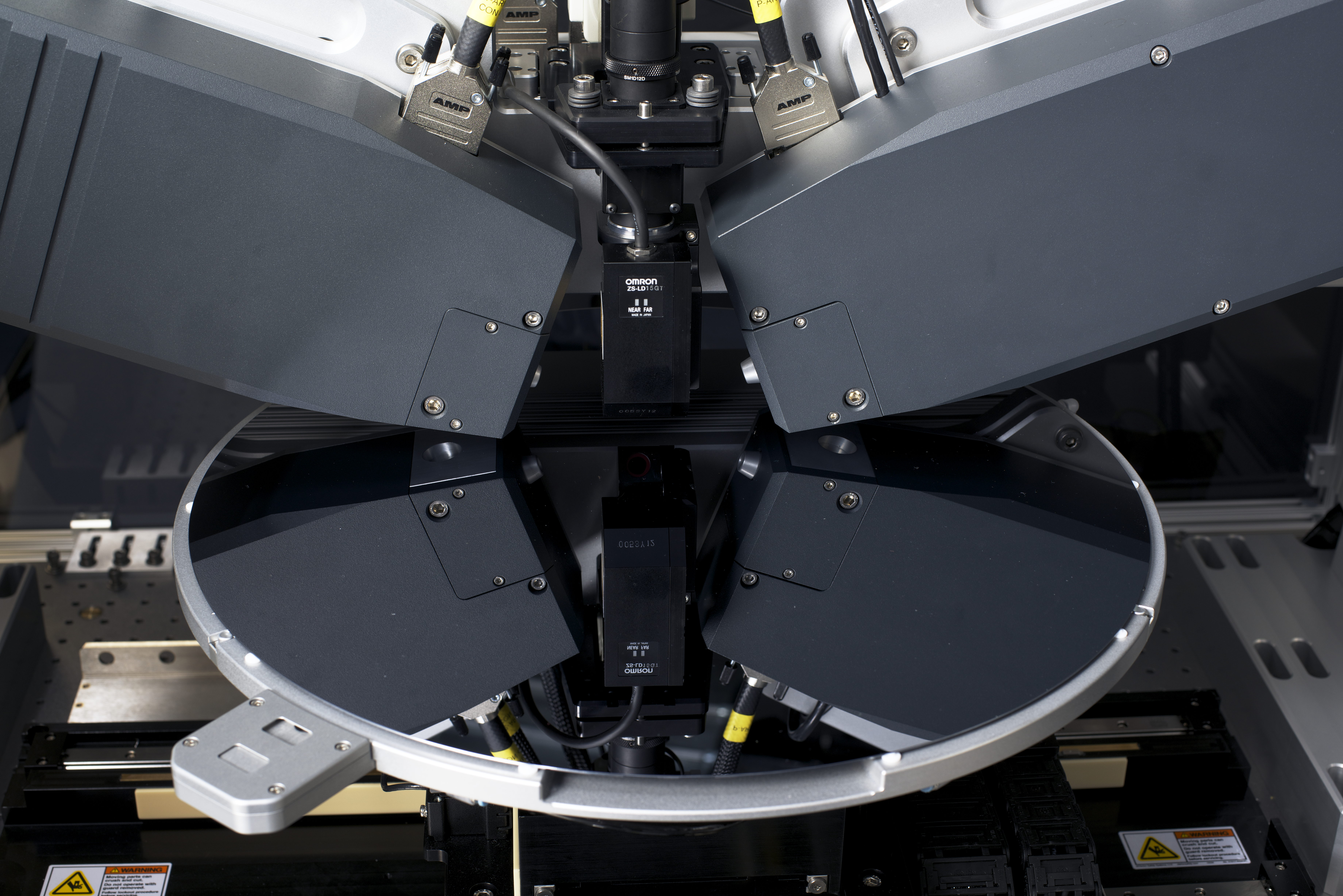
- Wafer size: On the chuck can be put several size and shape of wafers of 150/200/300/450 mm
- Auto focus module with Omron distance sensor
- Light source: Xenon lamp
- Fast spectrograph ensured with high resolution CCD detector
- Sample Stage with X-Y movement for:
- Mapping
- Multi-point measurements
- Single point measurements
- Automated Z movement for excellent focusing
- Pressure control unit for regulated high pressure and vacuum supplies
- Recipe-based operation, based on SEMI recommendations